ATmega328 Timers and Interrupts, Lecture notes of Microwave Engineering and Acoustics

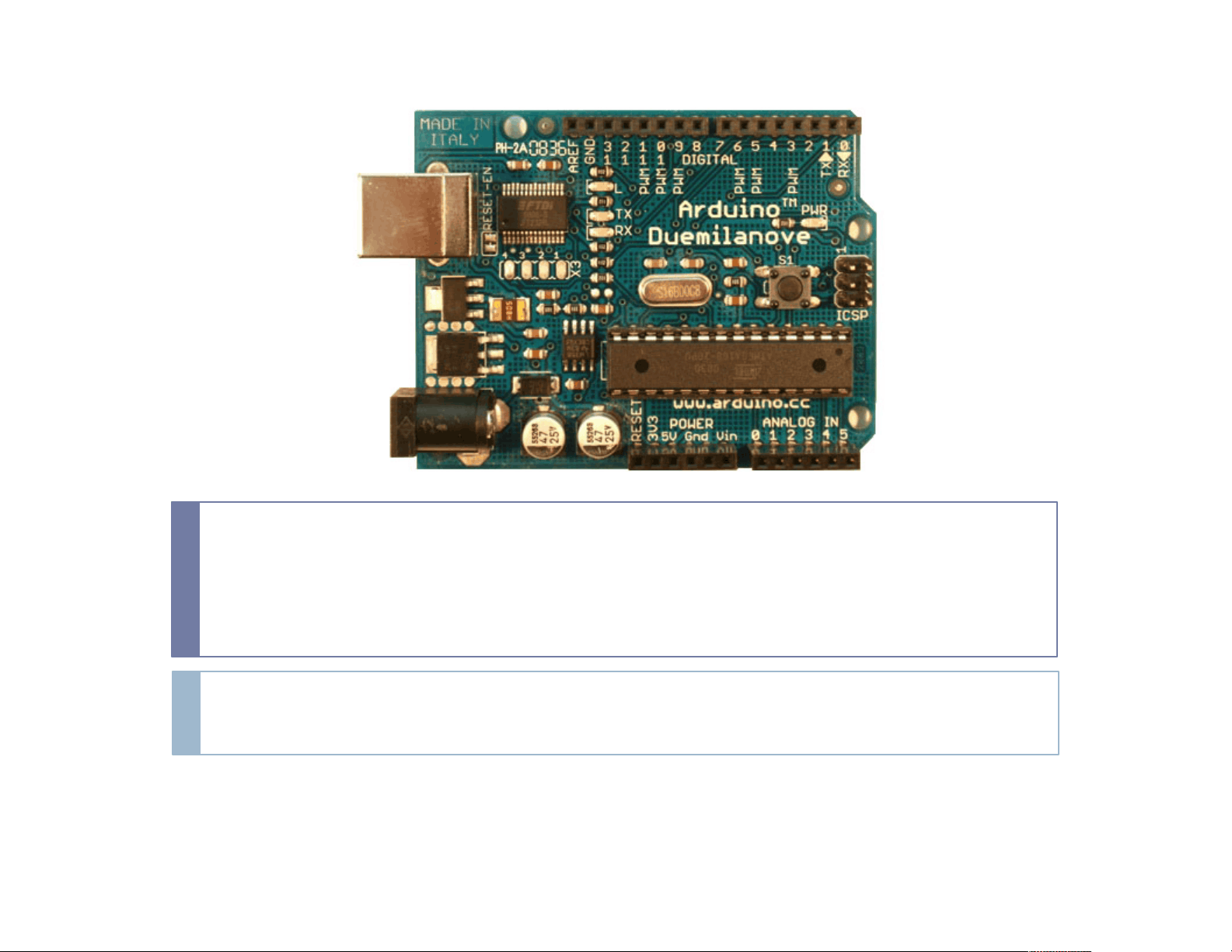
The ATmega328 Timers and Interrupts. It covers the digital and analog I/O pins, digital pin I/O functions, and interrupts. It also explains the interrupt model, interrupt vectors, and external interrupts. Additionally, it covers the Pin Change Mask Register 2, 8-bit Timer/Counter 0, and Timer/Counter Registers. a technical guide for students studying microcontrollers and embedded systems.

Typology: Lecture notes

2021/2022

Uploaded on 05/11/2023

ekaraj
ekaraj šŸ‡ŗšŸ‡ø

4.6

(30)

264 documents

1 / 48

Toggle sidebar

This page cannot be seen from the preview

Don't miss anything!

bg1
Lecture 6 – ATmega328 Timers
and Interrupts
CSE P567
pf3
pf4
pf5
pf8
pf9
pfa
pfd
pfe
pff
pf12
pf13
pf14
pf15
pf16
pf17
pf18
pf19
pf1a
pf1b
pf1c
pf1d
pf1e
pf1f
pf20
pf21
pf22
pf23
pf24
pf25
pf26
pf27
pf28
pf29
pf2a
pf2b
pf2c
pf2d
pf2e
pf2f
pf30

Partial preview of the text

Download ATmega328 Timers and Interrupts and more Lecture notes Microwave Engineering and Acoustics in PDF only on Docsity!

Lecture 6 – ATmega328 Timers

and Interrupts

CSE P

Arduino Digital and Analog I/O Pins

 Digital pins:

 Pins 0 – 7: PORT D [0:7]

 Pins 8 – 13: PORT B [0:5]

 Pins 14 – 19: PORT C [0:5] (Arduino analog pins 0 – 5)

 digital pins 0 and 1 are RX and TX for serial communication

 digital pin 13 connected to the base board LED

 Digital Pin I/O Functions

 pinMode( pin , mode )

 Sets pin to INPUT or OUTPUT mode

 Writes 1 bit in the DDRx register

 digitalWrite(pin, value)

 Sets pin value to LOW or HIGH (0 or 1)

 Writes 1 bit in the PORTx register

 int value = digitalRead(pin)

 Reads back pin value (0 or 1)

 Read 1 bit in the PINx register

Interrupts

 Allow program to respond to events when they occur

 Allow program to ignore events until the occur

 External events e.g.:

 UART ready with/for next character

 Signal change on pin

 Action depends on context

 # of edges arrived on pin

 Internal events e.g.:

 Power failure

 Arithmetic exception

 Timer ā€œtickā€

ATmega328 Interrupts (cont)

Interrupt Model

 When an interrupt event occurs:

 Processor does an automatic procedure call

 CALL automatically done to address for that interrupt

 Push current PC, Jump to interrupt address

 Each event has its own interrupt address

 The global interrupt enable bit (in SREG) is automatically cleared

 i.e. nested interrupts are disabled

 SREG bit can be set to enable nested interrupts if desired

 Interrupt procedure, aka ā€œinterrupt handlerā€

 Does whatever it needs to, then returns via RETI

 The global interrupt enable bit is automatically set on RETI

 One program instruction is always executed after RETI

Interrupt Model

 Interrupt hander is invisible to program

 Except through side-effects, e. g. via flags or variables

 Changes program timing

 Can’t rely on ā€œdead-reckoningā€ using instruction timing

 Must be written so they are invisible

 Cannot stomp on program state, e. g. registers

 Save and restore any registers used

 Including SREG

Interrupt Vectors

 Table in memory containing the first instruction of each

interrupt handler

 Typically at program address 0

Defined ISR’s

#define INT0_vect _VECTOR(1) /* External Interrupt Request 0 / #define INT1_vect _VECTOR(2) / External Interrupt Request 1 / #define PCINT0_vect _VECTOR(3) / Pin Change Interrupt Request 0 / #define PCINT1_vect _VECTOR(4) / Pin Change Interrupt Request 0 / #define PCINT2_vect _VECTOR(5) / Pin Change Interrupt Request 1 / #define WDT_vect _VECTOR(6) / Watchdog Time-out Interrupt / #define TIMER2_COMPA_vect _VECTOR(7) / Timer/Counter2 Compare Match A / #define TIMER2_COMPB_vect _VECTOR(8) / Timer/Counter2 Compare Match A / #define TIMER2_OVF_vect _VECTOR(9) / Timer/Counter2 Overflow / #define TIMER1_CAPT_vect _VECTOR(10) / Timer/Counter1 Capture Event / #define TIMER1_COMPA_vect _VECTOR(11) / Timer/Counter1 Compare Match A / #define TIMER1_COMPB_vect _VECTOR(12) / Timer/Counter1 Compare Match B / #define TIMER1_OVF_vect _VECTOR(13) / Timer/Counter1 Overflow / #define TIMER0_COMPA_vect _VECTOR(14) / TimerCounter0 Compare Match A / #define TIMER0_COMPB_vect _VECTOR(15) / TimerCounter0 Compare Match B / #define TIMER0_OVF_vect _VECTOR(16) / Timer/Couner0 Overflow / #define SPI_STC_vect _VECTOR(17) / SPI Serial Transfer Complete / #define USART_RX_vect _VECTOR(18) / USART Rx Complete / #define USART_UDRE_vect _VECTOR(19) / USART, Data Register Empty / #define USART_TX_vect _VECTOR(20) / USART Tx Complete / #define ADC_vect _VECTOR(21) / ADC Conversion Complete / #define EE_READY_vect _VECTOR(22) / EEPROM Ready / #define ANALOG_COMP_vect _VECTOR(23) / Analog Comparator / #define TWI_vect _VECTOR(24) / Two-wire Serial Interface / #define SPM_READY_vect _VECTOR(25) / Store Program Memory Read */

Interrupts

 Global interrupt enable

 Bit in SREG

 Allows all interrupts to be disabled with one bit

 sei() – set the bit

 cli() – clear the bit

 Interrupt priority is determined by order in table

 Lower addresses have higher priority

 ISR(vector) – Interrupt routine definition

 reti() – return from interrupt

 automatically generated for ISR

INT0 and INT

 External Interrupt Control Register:

 Sense Control (INT0 is the same)

INT0 and INT

 External Interrupt Mask Register

 If INT# bit is set (and the SREG I-bit is set), then interrupts are

enabled on pin INT#

 External Interrupt Flag Register

 Interrupt flag bit is set when a change triggers an interrupt

request

 Flag is cleared automatically when interrupt routine is executed

 Flag can be cleared by writing a 1 to it

PCINT[23:0]

 Pin Change Interrupt Control Register

 PCIE2 enables interrupts for PCINT[23:16]

 PCIE1 enables interrupts for PCINT[14:8]

 PCIE0 enables interrupts for PCINT[7:0]

 Pin Change Interrupt Flag Register

 PCIF# set if corresponding pins generate an interrupt request

 Cleared automatically when interrupt routine is executed

PCINT[23:0]

 Pin Change Mask Register 2

 Each bit controls whether interrupts are enabled for the

corresponding pin

 Change on any enabled pin causes an interrupt

 (Mask registers 1 and 0 are similar)