Download Electronic Component Selection and Testing for FSK Transmitter-Receiver System and more Exams Music in PDF only on Docsity!
TL/H/
LM1893/LM2893 Carrier-Current Transceiver
April 1995
LM1893/LM2893 Carrier-Current Transceiver≤
General Description
Carrier-current systems use the power mains to transfer in- formation between remote locations. This bipolar carrier- current chip performs as a power line interface for half-du- plex (bi-directional) communication of serial bit streams of virtually any coding. In transmission, a sinusoidal carrier is FSK modulated and impressed on most any power line via a rugged on-chip driver. In reception, a PLL-based demodula- tor and impulse noise filter combine to give maximum range. A complete system may consist of the LM1893, a COPS TM controller, and discrete components.
Features
Y (^) Noise resistant FSK modulation Y (^) User-selected impulse noise filtering Y (^) Up to 4.8 kBaud data transmission rate Y (^) Strings of 0’s or 1’s in data allowed Y (^) Sinusoidal line drive for low RFI
Y (^) Output power easily boosted 10-fold Y (^) 50 to 300 kHz carrier frequency choice Y (^) TTL and MOS compatible digital levels Y (^) Regulated voltage to power logic Y (^) Drives all conventional power lines
Applications
Y (^) Energy management systems Y (^) Home convenience control Y (^) Inter-office communication Y (^) Appliance control Y (^) Fire alarm systems Y (^) Security systems Y (^) Telemetry Y (^) Computer terminal interface
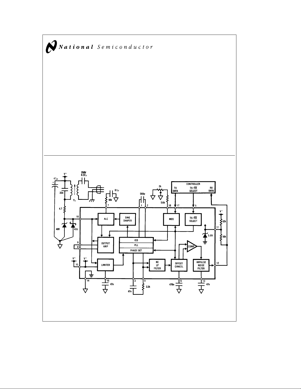
Typical Application
TL/H/6750– FIGURE 1. Block diagram of carrier–current chip with a complement of discrete components making a complete FOe125 kHz, fDATAe360 Baud transceiver. Use caution with this circuit–dangerous line voltage is present.
BI-LINE TM^ and COPS TM^ are trademarks of National Semiconductor Corp. ≤Carrier-Current Transceivers are also called Power Line Carrier (PLC) transceivers.
C1995 National Semiconductor Corporation RRD-B30M115/Printed in U. S. A.
Absolute Maximum Ratings
If Military/Aerospace specified devices are required, please contact the National Semiconductor Sales Office/Distributors for availability and specifications. Supply voltage 30 V Voltage on pin 12 55 V Voltage on pin 10 (Note 1) 41 V Voltage on pins 5 and 17 40 V 5.6 V DC zener current 100 mA
Junction temperature: transmit mode 150 ßC
receive mode 125 ßC
Electro-Static Discharge (120 pF, 1500X) 1KV
Maximum continuous dissipation, T Ae 25 ßC,
plastic DIP N (Note 2): transmit mode 1.66 W receive mode 1.33 W
Operating ambient temp. range b40 to 85ßC
Storage temperature range b65 to 150ßC
Lead temp., soldering, 7 seconds 260 ßC
Note:Absolute maximum ratings indicate limits beyond which damage to the device may occur. Electrical specifica- tions are not ensured when operating the device above guaranteed limits but below absolute maximum limits, but there will be no device degradation.
General Electrical Characteristics
(Note 3). The test conditions are: Va^ e18V and F (^) Oe125 kHz, unless otherwise noted. Test Design (^) Limit › (^) Parameter Conditions Typical Limit Limit Units (Note 4) (Note 5) 1 5.6 V Zener voltage, VZ Pin 11, IZe2 mA 5.6 5.2 V min. 5.9 V max. 2 5.6 V Zener resistance, RZ Pin 11, RZe(VZ@10 mAbV (^) Z@1 mA)/(10 mAb1 mA) 5 X 3 Carrier I/O peak survivable Pin 10, discharge 1 mF cap. charged to VOT 80 60 V max. transient voltage, V (^) OT thru k 1 X 4 Carrier I/O clamp voltage, VOC Pin 10, IOCe10 mA, RX mode 44 41 V min. 2N2222 diode pin 8 to 9 50 V max. 5 Carrier I/O clamp resistance, R 10 Pin 10, IOCe10 mA 20 X 6 TX/RX low input voltage, VIL Pin 5 1.8 0.8 V max. 7 TX/RX high input voltage, VIH Pin 5 (Note 9) 2.2 2.8 V min. 8 TX/RX low input current, IIL Pin 5 at 0.8 V b 2 b 20 mA min. 1 mA max. 9 TX/RX high input current, IIH Pin 5 at 40 V b 1 0 mA min. 10 b^4 10 mA max.
10 RXbTX switch-over time, TRT Time to develop 63% of full current drive thru pin 10 10 ms
11 TXbRX switch-over time, TTR 1 bit time, TBe1/(2FDATA). Time TTR is user 2 bit controlled with C (^) M, see Apps. Info.
12 ICO initial accuracy of FO TX mode, RO e^ 6.65 kX, CO e^ 560 pF 125 113 kHz min. F 0 e^ (F 1 a^ F 2 )/2 137 kHz max. 13 ICO temperature coefficient of FO TX or RX mode, (FOMAXbFOMIN)/(TJMAXbTJMIN) b 100 PPM/ßC
14 Temperature drift of FO TX or RX mode, b 40 sTJsTJMAX g2.0 g5.0 % max.
Transmitter Electrical Characteristics (Note 3). The test conditions are: Va^ e18 V and F Oe125 kHz
unless otherwise noted. The transmit center frequency is F (^) O , FSK low is F 1 , and FSK high is F 2. Test Design › Parameter Conditions Typical Limit Limit Limit (Note 4) (Note 5) Units 15 Supply voltage, Va, range Meets test 17 spec. at TJe 25 ßC and: 13 14 15 V min. l(F^1 [14V]bF 1 [18V])/F 1 [18V]lk0.01^40 24 23 V max. l(F^1 [24V]bF 1 [18V])/F 1 [18V]lk0. 16 Total supply current, IQT Pin 15. Pin 12 high. IQT is IQ through 52 79 mA max. pin 15 and the average current I (^) ODC of the Carrier I/O through pin 10 17 Carrier I/O output current, IO 100 X load on pin 10 70 45 mApp min. 18 Carrier I/O lower swing limit, VALC Pin 10. Set internally be ALC. 4.7 4.0 V min. 2N2222 diode pin 8 to 9 5.7 V max. 19 THD of IO (Note 6) Q of 10 tank driving 10X line 0.6 5.0 % max. 100 X load, no tank 5.5 9 % max. 20 FSK deviation, F 2 bF 1 (F 2 bF 1 )/([F 2 aF 1 ]/2) 4.4 3.7 % min. 5.2 % max. 21 Data In. low input voltage, VIL Pin 17 1.7 0.8 V max. 22 Data In. high input voltage, VIH Pin 17 (Note 9) 2.1 2.8 V min. 23 Data In. low input current, IIL Pin 17 at 0.8 V b 1 b 10 mA min. 1 mA max. 24 Data In. high input current, IIH Pin 17 at 40 V b 1 0 mA min. 10 b^4 10 mA max.
Typical Performance Characteristics (Va^ e18V, FO e^ 125 kHz, circuit ofFigure 1 , pin numbers for
LM1893)
Total Current Consumption, I (^) QT, vs Supply Voltage
Total Current Consumption, IQT, vs Junction Temperature
Chip Bias Current, iQ, vs Supply Voltage
Chip Bias Current, IQ, vs Junction Tempurature
Output Stage DC Current, I (^) ODC, vs Output Voltage
Output Stage DC Current, I (^) ODC, vs Junction Temperature
Transient Voltage Survival vs Pulse Time
Transmitter AC Output Current vs Junction Temperature
Transmitter Sinusoid THD vs Junction Temperature
ALC Voltage vs Junction Temperature
ICO Frequency vs Junction Temperature
Transmitter FSK Deviation vs Junction Temperature
TL/H/6750–
Typical Performance Characteristics (Continued)
Maximum Data Rate vs Junction Temperature
Receiver Sensitivity vs Junction Temperature
PLL Lock Range vs Junction Temperature and FO
PLL Capture & Lock Range vs Junction Temperature
Receiver Sensitivity vs PLL Lock Range and FO
Receiver Sensitivity vs PLL Lock Range and Loop Filter
Impulse Noise Filter Current vs Junction Temperature
Phase Detector Output Voltage vs Junction Temperature
Offset Hold Cap. Charge Currents vs Junction Temperature
Offset Hold Cap. Bias Current vs Junction Temperature
Data Out. Low Voltage vs Pull Down Current
Pin 7 Bias Voltage vs Junction Temperature
TL/H/6750–
Application Information (Continued)
TL/H/6750–
FIGURE 4. Block diagram of a CCT system with the boost and 5V supply options shown in dashed boxes
Application Information (Continued)
› Recommended^ Purpose Effect of making the component value:^ Notes Value (^) Smaller Larger
CO 560 pF Together, CO and RO Increases FO Decreases FO g5% NPO ceramic. Use low TC R (^) O 6.2 kX set ICO FO. Increases FO Decreases FO 2 k pot and 5.6 k fixed R. k5.6 k not recommended. l7.6 k not recommended. Poor FO TC with k5.6 k RO.
CF 0.047 mF PLL loop filter pole Less noise immune, higher More noise immune, lower Depending on RF value and f (^) DATA, more PLL stability. fDATA, less PLL stability. FO, PLL unstable with large RF 3.3 kX PLL loop filter zero PLL less stable, allows PLL more stable, allows CF. See Apps. Info. CF less CF. Less ringing. more CF. More ringing. and RF values not critical.
CC 0.22 mF Couples FO to line, Low TX line amplitude. Drives lower line Z. t250 V non-polar. Use 2CC CC and T 1 low-pass Less 60 Hz T 1 current. More 60 Hz T 1 current. on hot and neutral for max. attenuates 60 Hz. Less stored charge. More stored charge. line isolation, safety.
CQ 0.033 mF Tank matches line Z, Tank FO up or increase Tank FO down or decrease 100 V nonpolar, low TC, g10% bandpass filters, L of T 1 for constant FO. L of T 1 for constant FO. High large-signal Q needed. T 1 Use isolates from line, Smaller L: higher FO or Larger L: lower FO or Optimize for low FO line recommended and attenuates increase CC; decreased FO decrease CC; increased FO pull with control of FO TC XFMR transients. line pull. line pull. and Q.
CA 0.1 mF ALC pole Noise spikes turn ALC off. Slower ALC response. RA optional. ALC stable R (^) A 10 kX ALC zero Less stable ALC. More stable ALC. for CAt100 pF.
CL 0.047 mF Limiter 50 kHz pole, Higher pole F, more 60 Hz Lower pole F, less 60 Hz Any reasonably low TC cap. 60 Hz rejection. reject. FO attenuation? reject, more noise BW. 300 pF guarantees stability.
CM 0.47 mF Holds RX path VOS Less noise immune, shorter More noise immune, longer Low leakage g20% cap. VOS hold, faster VOS aqui- V (^) OS hold, slower VOS aqui- Scale with fDATA. sition, shorter preamble. sition, longer preamble.
CI 0.047 mF Rejects short pulses Less impulse reject, less More impulse reject, more CI charge time (/2 bit nom. like impulse noise. delay, more pulse jitter. delay, less pulse jitter. Must be k1 bit worst-case.
RC 10 kX Open-col. pull-up Less available sink I. Less available source I. RCt1.5 kX on 5.6 V
RZ 12 kX 5.6 V Zener bias Larger shunt current, Smaller shunt current, 1 kIZk30 mA recommended. more chip dissipation. less Va^ current draw. (Chip power-up needs 5.6 V)
ZT t44 V BV Transient clamp ZT failure, higher series ZT costly, lower series Recommend Zener rated k60 V peak R-excess peak V, Zener R gives enhanced for t500 W for 1 ms. and chip damage, transient clamp, less ruggedness. more ruggedness. R (^) T 4.7 X Transient I limit Damage ZT , pull up Va. Excessive TX attenuation. Carbon comp. recommended. D (^) T t44V BV Over-drive Clamp Failure on Transient Costly IRF 11DQ05 or 1N
RB 180 X Base bleed Faster, lower THD IO. Inadequate turn-off speed. Boost optional. QB F(b3 dB) Q (^) B Power NPN Boost gain device Excessive TJ and VSAT. More rugged, but costly. of l200 MHz. RB l^ 24 Ohm. RG 1.1 X Current setting R More IO, need higher hfe. Less IO, lower min. hfe. I (^) Oe 70 [(10aR (^) G)/R (^) G]^ mApp.
CB t 47 mF Supply bypass Transients destroy chip. Less supply spike. Va^ never over abs. max.
ZA 5.1V Stop ALC charge Excess ALC ALC RX charging ZA optional - 5.1V in RX mode current flow not inhibited over TJ g20% low leakage type
FIGURE 5. A quick explanation of the external component function using the circuit ofFigure 4. Values given are for Va^ e 18 V, FO e^ 125 kHz, fDATA e^ 360 Baud (180 Hz), using a 115 V 60 Hz power line
Component Selection
Assuming the circuit ofFigure 4 is used with something oth- er than the nominal 125 kHz carrier frequency, 180 Hz data rate, 18V supply voltage, etcetera, the component values listed inFigure 5 will need changing. This section will help direct the CCT designer in finding the required component values with emphasis placed on look-up tables and charts. It is assumed that the designer has selected values for carrier center frequency, F (^) O; data rate, f (^) DATA; supply voltage, Va; power line voltage, V (^) L; and power line frequency, F (^) L. If one or more of those parameters is not defined, one may read the data sheet and make an educated guess. Maxims to keep in mind, based on CCT electrical perform-
ance considerations only, are: 1) the higher the F (^) O the bet- ter, 2) the lower the maximum data rate the better, and 3) the more time and frequency filtering the better. UseFigure 5 as a quick reference to the external compo- nent function.
THE TRANSMITTER
CO Central to chip operation is the low TC of F (^) O emitter-cou- pled oscillator. With proper CO, the FO of the 2VBE ampli- tude triangle-wave oscillator output may vary from near DC to above 300 kHz. While CO may have any value, CO should
Component Selection (Continued)
C C
Capacitor C (^) C ’s primary function is to block the power line voltage from T 1 ’s line-side winding. Also, C (^) C and T 1 ’s line- side winding comprise a LC highpass filter. The self-induc- tance of T 1 is far too low to support a direct line connection. CC must have a low enough impedance at FO to allow T 1 to drive transmitted energy onto the line. To drive a 14X power line, the impedance of C (^) C should be below 14X. UseFigure 9 to find the reactive impedance of CC to check that it is less than the line impedance. Then checkFigure 10 to see that the power line current is small enough to keep T 1 well out of saturation; the recommended transformers can withstand a 10 Amp-turn magnetizing force (1 Amp through the worst-case 10 turn line-side winding). Caution is required when choosing C (^) C to avoid series reso- nance of the series combination of C (^) C , the transformer in- ductance, and the reflected tank impedance. The low resist- ance of the network under series resonance will load the line, possibly decreasing range. For your particular line cou- pling circuit, measure for series resonance using some ex- pected line impedance load.
R (^) B This base-bleed resistor turns Q (^) B off quickly - important since the amplifier output swing is about 200V/ms. An RB below about 24X will conduct excessive current and over- load the chip amplifier and is not recommended.
TL/H/6750– FIGURE 9. CC’s impedance should be, as a rule-of-thumb, smaller than the lowest expected line impedance
RG This resistor, in parallel with the internal 10X resistor, fixes the current gain of the output amplifier, and so the output current amplitude.Figure 11 gives output current and mini- mum AC current gain hfe for QB when RG is used to boost output current.
Q (^) B The boost gain transistor QB must be fast. Double-diffused devices with 50 MHz F (^) T ’s work, slower transistors (epi-base types) do not preserve a sinusoidal waveform when FO is high or will cause the output amp. to oscillate. Q (^) B must have a certain minimum hfe for given boost levels, as shown in Figure 11 .Figure 12 shows the power QB must dissipate continuously operating with a shorted output. BV (^) CER (R e RB) must be 60V or greater and QB must have adequate SOA for transient survival.
ZT Unfortunately, potentially damaging transient energy passes through transformer T 1 onto the Carrier I/O pin (instanta-
neous power of greater than 1 kW has been measured us- ing the recommended transformers). For self protection, the Carrier I/O has an internal 44V voltage clamp with a 20X series resistance. A parallel low impedance 44V external transient suppression diode will then conduct the lion’s share of any current when transients force the Carrier I/O to a high voltage.
TL/H/6750– FIGURE 10. The AC line-induced current passed by CC
TL/H/6750– FIGURE 11. Output amplifier current and required min. QB hfe versus gain-setting resistor RG
TL/H/6750– FIGURE 12. Boost transistor power dissipation versus amplifier output current ZT must be used unless some precaution is taken to protect the Carrier I/O pin from line transients or transients caused when stored line energy in CC is discharged by the random phase of power line connection and disconnection. Worst case, C (^) C may discharge a full peak-to-peak line voltage into the tuned circuit. Another way to reduce the need for ZT is by placing another magnetic circuit in the signal path that relies on a high, but easily saturated, permeability to couple a primary and secondary winding - a toroidal transformer for example. Toroids cost more than Z (^) T. Use an avalanche diode designed specifically for transient suppression – they have orders of magnitude higher pulse
Component Selection (Continued)
power capability than standard avalanche diodes rated for equal DC dissipation. Metal oxide varistors have not proven useful because of their inferior clamping coefficient and are not recommended. Specifications for an example minimum diode are given inFigure 13. Breakdown Voltage 44–49V @^ 1 mA Maximum Leakage 1 mA @^ 40V Capacitance 300 pF @^ BV Maximum Clamp Voltage 64.5V @^ 7.8A Peak Non-Repetitive Pulse Power 10 kW for 1 ms (REA Standard Exponential Pulse) Surge Current 70A for 1/120s FIGURE 13. Key specifications for a recommended transient suppressor ZT available from General Semiconductor, 2001 West Tenth Place, Tempe, AZ 85281, 602–968-3101, part no. SA40A
R (^) T RT acts as a voltage divider with ZT, absorbing transient energy that attempts to pull the Carrier Input pin above 44V. Make the resistor a carbon composition 1/4W. When exper- iments discharging C (^) C charged to the peak-to-peak 620V AC thru a 1X power line were carried out, film resistors blew open-circuit.
D (^) T This Schottky diode is placed in parallel with the CCT chip’s substrate diode to pass the majority of the current drawn from ground when the Carrier Input or Carrier Output is pulled below ground by a larger-than-twice-the supply-swing on the tank. Note that Z (^) T is in parallel with the substrate diode, but is ineffective due to its high forward voltage drop and high diffusion capacitance caused by its low forward speed. Tests proved that a 1N5818 kept a receive-path functional with a 20X boost transmitter with a 7:1 transform- er attempted to swing the receiver’s Carrier I/O to g100V (300 mA peak ground current in the receiver). Without D (^) T, the receiver momentarily stops functioning at a 100 times lower ground current. This diode is not needed if the Carrier I/O never swings below ground. If your CCT systems all run on the same regulated voltage with all matched transformers and turns ratios, it is not needed. Otherwise, it is.
THE RECEIVER The receiver and transmitter share components CC , T 1 , CQ, R (^) T , ZT , CO, RO, and peripheral supply and bias components that are not in need of change for RX mode operation. Val- ues for the balance of the components are now found.
Line-Frequency Rejection To use the ultimate sensitivity of the device, fully 110 dB of 115 V, 60 Hz attenuation is required between the line and the limiter amplifier output. Using the circuit topology ofFig- ure 4 , the combined attenuation of the CC /T 1 highpass, the tuned transformer, and the bandpass filter attenuation of the limiter amplifier give far more line rejection than the above-stated minimum. However, if some other CCT line coupling circuit is used, line rejection will become important to the system designer. Receiver input power supply rejection (PSRR) and common- mode rejection (CMRR) are one-in-the-same using the sup- ply-referenced signal input ofFigure 4. Ripple swings both
differential inputs of the Norton amp. equally, while the sin- gle-ended input signal swings only the positive input. Overall PSRR consists of the input CMRR (set by the input stage component matching) and the ripple-frequency attenuation of the input amplifier bandpass response that passes carrier frequency but stops low frequencies. A typical 1% resistor and 1 mV n-p-n mirror offsets give 26 dB of attenuation, the bandpass gives 54 dB 120 Hz attenuation, for an overall 80 dB PSRR to allow tens of volts of ripple before impacting ultimate sensitivity.
CC A value was chosen earlier. Knowing T 1 ’s secondary induc- tance allows a check of LC line attenuation usingFigure 14.
C (^) L The Norton input limiter amplifier has a bandpass filter for enhanced receiver selectivity, noise immunity, and line fre- quency rejection. The nominal response curve for FO e^50 kHz is shown inFigure 15. The 300 kHz pole is fixed. The 50 kHz pole is set by CL ’s value. After CL is found, the resulting line frequency attenuation is found for the bandpass filter. UseFigure 15 to find a CL value given for FO. The approxi- mate line frequency attenuation of the bandpass filter may then be found inFigure 16 .Figure 15 returns a value for CL 33% larger than nominal, giving a low frequency pole 33% low to allow for component tolerances.
TL/H/6750– FIGURE 14. The 60 Hz line rejection of the highpass filter made up of CC and T 1 ’s line-side winding (neglecting capacitive coupling)
TL/H/6750–
TL/H/6750– FIGURE 15. Given FO, CL is found. Also shown is the input amplifier’s small signal amplitude response
Component Selection (Continued)
TL/H/6750– FIGURE 20. Size CM assuming a 2 bit-time receive bias time
C (^) I The impulse noise filter integrator capacitor CI is used to disallow the passage of any pulse shorter than the integra- tor charge time. That charge time, set to a nominal (/2 bit time, is the time required for a g 50 mA charge current to swing C (^) I over a 2 V (^) BE range. Charge time under worst case conditions must never be greater than a bit time since no signal could then pass. Using a g10% capacitor, full junc- tion temperature range, and full specified current range, a maximum nominal charge time of (/2 bit is recommended. Figure 21 gives CI versus data rate under those conditions.
R (^) C The collector pull-up resistor is sized to supply adequate pull-up current drive and speed while preserving adequate output low current drive.
TL/H/6750– FIGURE 21. Impulse noise filter cap. CI versus FDATA where the charge time is (/2 bit time
ZA
The 5.1V silicon zener diode ZA is required when a short RX-to-TX switch-over time is needed at the same time that the chip is operating in the RX mode with a pin 10 input signal swing approaching or exceeding twice the supply voltage. Predominant causes of these large swings imping- ing on the RX input are: 1) a transmitter’s supply voltage higher than the receiver’s supply voltage, 2) a TX and RX pair that are electrically close, or, 3) a higher RX T 1 step-up turns ratio than the TX T 1 step-down ratio. Normally, when in the RX mode with small incoming signal on pin 10, the ALC remains off with pin 7 at a 6V (V (^) Zb2V (^) BE) bias voltage. CA is then charged to 6V. TX mode may then be selected with 6V on CA allowing 100% TX power to pump T 1 ’s tuned circuit, and so the AC line, quickly for fast RX-to-TX switch time. As TX output swing increases so that pin 10 swings below VALC (4.7V typically), that ALC activates to charge CA to about 6.6V to reduce TX output drive. However, if in the RX mode pin 10 ever swings below VALC, CA will charge to above 6.6V. Now, when the TX mode is selected with C (^) A at 6.6V, somewhere from 0 to 100% TX output drive is available to pump T 1 ’s tuned circuit resulting in a slower rising line signal - effectively reducing the RX-to-TX switch time. Use a 5.1V Z (^) A driven by a 0 to 0.8V logic low signal to guarantee over-temp. operation. R (^) A must be in series with ZA to limit current flow and should never fall below 1 kX. If R (^) A is less than 1 kX, then put a 2 kX resistor in series with Z (^) A. Logic high voltages above 10V will cause current flow into pin 7 that must be limited to 1 mA (with RA or a series R).
Breadboarding Tips
During CCT system evaluation, some techniques listed be- low will simplify certain measurements.
- Use caution when working on this circuit - dangerous line voltages may be present.
- When evaluating PLL operation, offset cancel circuit op- eration, and loop filter values, use the filter ofFigure 22 to view the demodulated signal minus the 2FO and noise components. This filter models the RC lowpass filter on chip.
TL/H/6750– FIGURE 22. Circuit to view the differential demodulated data signal, minus the noise and 2FO components, conveniently with a single-ended gain-of-one output
Breadboarding Tips (Continued)
- When evaluating CCT system noise performance on a real power line, it is desirable to vary the signal ampli- tude to the receiver. This is not easy. An in-line line- proof L-pad is fine except that the line impedance is un- known and variable and so the L-pad will rarely match. Instead, the power output of a chip transmitter may be controlled using the circuit ofFigure 23. This circuit con- trols the ALC.
- It is sometimes desirable to place impulse noise on the line. A simple light dimmer with a 100 W light bulb load produces representative impulse noise.
- Do not allow peak currents of over 1 A through the 5.6 V Zener. In other words, don’t short charged capacitors into this low-impedance device. Take care not to mo- mentarily short pins 10 and 11 - chip damage may result.
- Figure 24 shows some typical signals beginning with se- rial data transmitted to received signal.
Tuning Procedure
This procedure applies to circuits similar toFigure 4 LM or LM2893 circuit.
First, trim F (^) O by putting the chip in the TX mode, setting a logical high data input, and measuring the TX high frequen- cy, 1.022 F (^) O, on the Carrier I/O using these steps:
- Take pin 17 to a logic low.
- Take pin 5 to a logic high.
- Place a counter on pin 10.
- Adjust R (^) O on pin 18 for F e^ 1.022FO.
Second, the line transformer is tuned. The chip is placed in the TX mode, a resistive line load is connected to disable the ALC by reducing tank voltage swing below its limit. FSK data is then passed through the tank so that the tank enve- lope may be adjusted for equal amplitude for high and low data frequency.
- Take pin 5 to a logic high.
- Place a logic-level square wave at or below the receiver’s maximum data rate on pin 17.
- Temporarily place a 330 X resistor across the tank.
- Place a scope on pin 10.
- Adjust the transformer slug for the least envelope modu- lation.
In lieu of the 330 X resistive load, T 1 may be coupled to the power line to better simulate actual load and tank pull condi- tions during tank tuning. Alternatively, a passive network
representing an average line impedance may be connected to the line side of T 1. The circuit ofFigure 23 should then be used to defeat the leveling effect of the ALC.
TL/H/6750– FIGURE 23. A means of transmitter output amplitude control is shown
Thermal Considerations
It is desirable to place the largest possible signal on the power line for maximum range, limited only by the chip pow- er dissipation and maximum junction temperature T (^) J. The falling output power at elevated TJ allows a more optimal power output - high power at low T (^) J and lower power at high T (^) J for chip self-protection. However, it is still possible to exceed the maximum TJ within the specified ambient tem-
perature limit (TA e^85 ßC) under worst case conditions of
100% TX duty cyle, high supply, shorted load, poor PC board layout (with small copper foil area), and an above nominal current part. Under those conditions, a part may
dissipate 2140 mW, reaching a TJ e^170 ßC worst-case (ad-
mittedly a rare occurrence). Proper system design includes the measurement or calculation of T (^) J max. to guarantee function under worst-case operation. Like all devices with failure modes modeled by the Arrhenius model, the high chip reliability is further enhanced by keeping the die tem- perature mercifully below the absolute maximum rating. A direct method of measuring operating junction tempera- ture is to measure the V (^) BE voltage on pin 18, which is al- ways available under all operating modes. The graph ofFig- ure 25 may be used to find TJ, knowing VBE at the operating
point in question and VBE at TA e^ TJ e^25 ßC. VBE is found
by powering up a chip (in RX mode) that has been dissipat- ing zero power at some T (^) A for some time and measuring
VBE in less than 1 s (for better than 5ßC accuracy).
Alternately, T (^) J may be calculated using: TJ e^ TA a^ iJAP (^) D (1)
where iJA is 75ßC/W for the plastic (N) package using a
socket. That iJA value is for a high confidence level; nomi-
TL/H/6750–
FIGURE 24. Oscillogram revealing signals at several important nodes under weak signal (0.5 mVRMS) conditions with SCR spikes on an otherwise quiet 115 V, 60 Hz power line. The signals are: 1) transmitted data, 2) RX carrier on the tuned transformer, 3) demodulated signal from the PLL after passing thru circuit ofFigure 22 , 4) signal after RC lowpass, 5) data at impulse noise filter integrator, and 6) received data. Horizontal scale is 10 ms per div.
Power Line Impedance (Continued)
TL/H/6750–29 TL/H/6750–30 (^) TL/H/6750– FIGURE 27. Complex-plane plots of measured 115V, 60 Hz line impedance where ZL e^ RL a^ jX (^) L
Power Line Attenuation
The wiring in most US buildings is a flat 3 conductor cable called Amerflex, BX, or Romex. All referenced line imped- ances refer to hot-to-neutral impedances with a grounded center conductor. The cable has a 100 X characteristic im- pedance, a 125 kHz quarter-wavelength of 600 m (250 m at 300 kHz), and a measured 7 dB attenuation for a 50 m run with a 10 X termination. Generally, line loads may be treat- ed as lumped impedances. Instrument line cords exhibit about 0.7 mH and 30 pF per meter.
Limited tests of CCT link range using this chip show exten- sive coverage while remaining on one phase of a distribu- tion transformer (100’s of m), with link failure often occuring across transformer phases or through transformers unless coupling networks are utilized. Total line attenuation allowed from full signal to limiting sensitivity is more than 70 dB. Typically, signal is coupled across transformer phases by parasitic winding capacitance, typically giving 40 dB attenu- ation between phased 115 V windings. Coupling capacitors may be installed for improved link operation across phases. Power factor correcting capacitor banks on industrial lines or filter capacitors across the power lines of some electronic gear short carrier signal and should be isolated with induc- tors. Increasing range is sometimes accomplished by elect- ing to install the isolating inductors (Figure 28 ) and coupling capacitors, as well as by electing to use the boost option. Frequency translating or time division multiplexed repeaters will also increase range.
TL/H/6750– FIGURE 28. An isolation network to prevent: 1) noise from some device from polluting the AC line, and 2) to stop some low impedance device (measured at Fo) from shorting carrier signal. Component values given as an example for Foe125 kHz on residential power lines
The Coupling Transformer
The design arrived at for T 1 is the result of an unhappy compromise - but a workable one. The goals of 1) building
T 1 with a stable resonant frequency, FQ, that is little affect- ed by the de-tuning effect of the line impedance ZL, and of
- building a tightly line-coupled transformer for transmitted carrier with loose coupling for transients, are somewhat mu- tually exclusive. The tradeoffs are exposed in the following example for the CCT designer attempting a new boost-ca- pable, or different core, transformer design. The compromises are eased by separating the TX output and RX input in the LM2893. An untuned TX coupling trans- former with only core coupling (not air-coupled solenoid windings) would employ a high permeability, high magnetic field, low loss, square saturating, toroidal core. The reso- nant RX path would be isolated from line-pull problems by a unilateral amplifier that operates at line voltages with much more than 110 dB of dynamic range, or by a capacitively coupled pulse transformer driving a unilateral amplifier and filter, for increased selectivity. See the LM2893-specific ap- plications section. For a LM1893-style transformer application, first, choose the turns ratio N based on an estimated lowest ZL likely encountered, Z (^) LN.Figure 29 shows graphically how N af- fects line signal. N should be as large as possible to drive Z (^) LN with full signal. If T 1 has an unloaded Q, Q (^) U, of well less than 35, a guess of N somewhat high should be used and later checked for accuracy. The recommended transformers have secondary taps giving a choice of Ne7.07, 10, and 14.1 (nominally) for driving Z (^) LN ’s of 14, 7.0, and 3.5 X re-
spectively (at T J e^25 ßC, Va e^ 18V, and Q U e^ 35).
The resonating inductance of the tuned primary, L 1 , is sought. Note that, while standard transformer design gives a transformer self-inductance with an impedance at operating frequency well above load impedance, the tuned transform- er requires a low L 1 for adequate QU and minimum line pull. Result: relatively poor mutual coupling.
L 1 e^
R
2 qFOQ
It is known that resonant frequency FQ e^ FO and some minimum bandwidth, or maximum Q, will be required to pass signal under full load conditions.
L 1 e^
RQ ll lZ LNl
2 q FOQ (^) L
lZ^ LNl is the reflected ZLN, QL is the loaded Q, and parallel
resistance R (^) Q models all transformer losses and sets Q (^) O.
R Q ll lZLNl is found knowing that it absorbs full rated power.
The Coupling Transformer (Continued)
TL/H/6750– FIGURE 29. Impressed line voltage for a given ZL for each of the 3 taps available on the recommended transformers
P (^) OeI (^) OVOe
I OPP
2(bVALCaVa)
e (b4.7aVa)I (^) O 4
where I (^) O is in amps peak-to-peak at an elevated T (^) J
P (^) O e^
(18 b^ 4.7) 0. 4
e (^) 0.200 W (6)
R Qll lZ LNl e^
VO^2
P O
e (bVALC a^ Va) 02 I (^) O
e (^442) X (7)
R (^) Q is found using ZLN and the value for N found when as- suming Q (^) U e^ 35.
lZLNl e^ N^2 Z^ LN e^ (7.07)^2 13.9^ e^695 X^ (8)
RQ e^
RQll lZ LNl
b
lZLNl
e
b
e (^1210) X (9)
RQS e^
R Q
1 a Q (^) U^2
e
1 a 35 2
e (^1) X (10)
Only Q (^) L remains to be found to calculate L 1. Q (^) L is related to the b3 dB (half-power) bandwidth by
QL e^
BW (% of FO)
An iterative solution is forced where line pull, DFQ, must be guessed to find QL and L 1. L 1 is then used to check the line pull guess; a large error requires a new guess. Try a BW of 8.7% - that is 4.4% for deviation, 1% for TC of F (^) O, and 3.3% for DF (^) Q - giving Q (^) L e 11.5.
L 1 e^
2 q c^ 125 000 c^ 11.
e (^) 49.0 mH (12)
Knowing the core inductance per turn, L, and L 1 , the num- ber of turns is found.
T 1 e
L 1
L
e
49.0 mH 20 nH/T
e 49 (/2 turns (13)
T is normally an integer, but these transformers require so few turns that half-turns are specified, remembering that the remaining (/2 turn is completed on the P.C. board and is loosely coupled. The secondary turns are calculated
T 2 e^
T 1
N
e
e (^) 7.00 e (^) 7 turns (15)
giving an L 2 of 0.98 mH. Note that the recommended 125 kHz transformer mirrors these specifications. The resonat- ing capacitor is
C (^) Q e^
(2qFQ) 2 L 1
e (^) 33.1 c 10 b^9 e (^) 33 nF (16)
Line pull DFQ was calculated (reference 3) for a ZL magni-
tude of 14X and up with any phase angle from b 90 ß to 90ß.
DF (^) Q was 6.4% - well above the 3.3% estimate. Referring to (11), an 11.8% bandwidth is required, forcing L 1 to be re- duced to reduce Q. That fix was not implemented; some signal attenuation under worst-case drift and DFQ is al- lowed. L 1 is already so small that the 31 gauge winding conducts a (/4 A (^) RMS circulating current.
Line Carrier Detection
While the addition of a carrier detection circuit (for a mute or squelch function) will only decrease receiver ultimate sensi- tivity, there is sometimes good reason to employ it to free the controller from watching for RX signal when no carrier is incoming, or to employ it to reduce the probability of line collisions (when multiple transmitters operate simultaneous- ly to cause one or more transmissions to fail). Unless the detector is heavily filtered or uses a high carrier amplitude threshold, there will be false outputs that force the controller to have Data Out data checking capability just as is required when using no carrier detector. If false triggering is mini- mized, the probability of line collisions is increased due to the inability to sense low carrier amplitudes and because of sense delay. The property of the LM1893 to change output state infrequently (although the polarity is undefined) when in the RX mode, with no incoming carrier, reduces the desire to implement carrier detection and preserves the full ulti- mate sensitivity. Also, many impulse-noise insensitive trans- mission schemes, like handshaking, are easily modified to recover from line collisions. Regarding this, it should be stated that for very complicated industrial systems with long signal runs and high line noise levels, it is probably wise to use a protocol which is inherent- ly collision free so that no carrier detect hardware or soft- ware is needed. A token passing protocol is an example of such a system. Figure 30 shows a low cost carrier amplitude detection cir- cuit.
Audio Transmission
The LM1893 is designed to allow analog data transmission and reception. Base-band audio-bandwidth signals FM modulate the carrier passing through the tuned transformer (placing a limit on the usable percent modulation) onto the power line to be linearly demodulated by the receiver PLL. Because the receiver data path beyond the phase detector will pass only digital signal, external audio filtering and am- plification is required.Figure 31 shows a simple audio trans- mitter and receiver circuit utilizing a carrier detection mute circuit. A single LM339 quad. comparator may be used to build the carrier detect and mute. Filter bandwidth is held to a minimum to minimize noise, especially line-related corre- lated noise.
Communication and System
Protocols
The development of communication and system protocols has historically been the single most time consuming ele- ment in design of carrier current systems. The protocols are defined as the following: 1.Communication protocol : a software method of encoding and decoding data that remains constant for every transmis-
Communication and System
Protocols (Continued)
carrier current applications since they do not have the intelli- gence needed to distinguish between real messages and noise induced phantoms.
The difficulty in designing special protocols arises out of the special nature of the AC line, an environment laden with the worst imaginable noise conditions. The relatively low data rates possible over the AC line (typically less than 9600 baud) make it even more imperative that systems utilize the most sophisticated means available to ensure network effi- ciency.
With these facts in mind, the designer is referred to a publi- cation intended to aid in the development of carrier current systems. This is literature ›570075 The Bi-Line Carrier Cur- rent Networking System, a 200 pp. book that functions as the ‘‘bible’’ of Bi-Line system design. It has sections on LM1893 circuit optimization, protocol design, evaluation kit usage, critical component selection, and the Datachecker/ DTS case study.
Basic Data Encoding (please refer to the pre-
viously mentioned publications for advanced techniques)
At the beginning of a received transmission, the first 0 to 2 bits may be lost while the chip’s receiver settles to the DC bias point required for the given transmitter/receiver pair carrier frequency offset. With proper data encoding, dropped start bits can be tolerated and correct communica- tion can take place. One simple data encoding scheme is now discussed.
Generally, a CCT system consists of many transceivers that normally listen to the line at all times (or during predeter- mined time windows), waiting for a transmission that directs one or more of the receivers to operate. If any receiver finds its address in the transmitted data packet, further action such as handshaking with the transmitter is initiated. The receiver might tell the transmitter, via retransmission, that it received this data, waiting for acknowledgement before act- ing on the received command. Error detecting and correct- ing codes may be employed throughout. The transmitter must have the capability to retransmit after a time if no re- sponse from the receiver is heard - under the assumption that the receiver didn’t detect its address because of noise, or that the response was missed because of noise or a line collision. (A line collision happens when more than 1 trans- mitter operates at one time - causing one or more of the communications to fail). After many re-transmissions the transmitter might choose to give up. Collision recovery is achieved by waiting some variable amount of time before re-
transmission, using a random number of bits delay or a de- lay based on each transmitter’s address, since each trans- ceiver has a unique address. An example of a simple transmission data packet is shown inFigure 32. The 8 bit 50% duty-cycle preamble is long enough to allow receiver biasing with enough bits left over to allow the receiver controller to detect the square-wave that signals the start of a transmission. If there had been no transmission for some time, the receiver would simply need to note that a data transition had occurred and begin its watch for a square-wave. If the receive controller detected the alternating-polarity data square-wave it would then use the sync. bit to signal that the address and data were imme- diately following. The address data would then be loaded, assuming the fixed format, and tested against its own. If the address was correct, the receiver would then load and store the data. If the address was not correct, either the transmis- sion was not meant for this receiver or noise has fooled the receiver. In the former case, when the transmission was not meant for the receiver, the controller should immediately return to watching the incoming data for its address. If the later case were true, then the receive controller would con- tinue to detect edges, tieing itself up by loading false data and being forced to handshake. The square-wave detection and address load and check routines should be fast to mini- mize the time spent in loops after being false-triggered by noise. If the controller detects an error (a received data bit that does not conform to the pre-defined encoding format) it should immediately resume watching the LM1893’s Data Out for transmissions, the next bit would be shifted in and the process repeated. A line-synchronous CCT system passing 3 bits per half-cy- cle may replace the long 8 bit preamble and sync pulse with a 2 bit start-of-transmission bias preamble. The receive con- troller might then assume that preamble always starts after bit 1 (the first bit after zero-crossing) so that any data tran- sition at a zero crossing must be the start of the address bits and is tested as such. The line synchronous receiver oper- ates with a simpler controller than an asynchronous system. Discussion has assumed that the controller has always known when the Data Out is high or low. The controller must sample at the proper time to check the Data Out state. Since noise shows itself as pulse width jitter, symmetrically placed about the no-noise switch-points, optimum Data Out sampling is done in the center of the received data pulse. The receive data path has a time delay that, at low data rates, is dominated by the impulse noise filter integrator and is nominally (/2 bit. At a 2 kHz data rate, an additional delay of approximately (/10 bit is added because of the cumulative delay of the remainder of the receiver.Figure 33 shows that Data Out sampling occurs conveniently at the transmitted
TL/H/6750– FIGURE 32. A simple encoded data packet, generated by the transmit controller is shown. The horizontal axis is time where 1 bit time is 1/(2fDATA)
Basic Data Encoding (Continued)
TL/H/6750– FIGURE 33. Operating waveforms of a line- synchronized transceiver pair are shown. The diagram shows how the transmitted data transitions may be used as received data sampling points
data edges for the line synchronous data transmission scheme mentioned in the previous paragraph. With the asynchronous system suggested, the receive controller must sample the Data Out pin often to determine, with sev- eral bits of accuracy, where the square-wave data tran- sitions take place, average their positions assuming a known data rate, and calculate where the center of the data bits are and will continue to be as the address and data are read. A long preamble is helpful. Software that continuously updates the center-of-bit time estimate, as address and data are received, works even better. Alternatively, a coding scheme employing an embedded clock can be used.
LM2893 Application Hints
The LM2893 is intended for advanced applications where special circuitry is used in the transmit and receive paths. The LM2893 makes this possible by featuring separate transmit output and receive input pins.
Examples of enhancements that can be added to the basic LM1893/2893 circuit include separate transmit and receive windings on the coupling transformer, high quality ceramic or LC filters in the receive path, and simple impulse noise blanking circuits.
In many applications, the additional performance to be gained outweighs the extra cost of the additional circuitry. More than likely, high performance industrial applications such as building energy management will fit into this catego- ry, since they require the utmost in reliability.
Because of the specialized nature of individual LM2893 ap- plications, it is not possible to give one circuit that will satisfy all requirements for performance and cost effectiveness. Therefore no specific application examples will be given. Instead the subsequent text describes in general terms the types of circuits that can be used to increase performance along with their advantages and disadvantages. It is intend- ed to be a springboard for ideas.
LM2893 COUPLING NETWORKS
The main disadvantages of the typical LM1893 coupling network are that it functions as the bandpass filter, has loose coupling between primary and secondary, and has a single secondary. The LM1893 coupling network was de- signed this way mainly because of the restraint that the car- rier input and output are tied together.
Because the coupling transformer is used as a filter, the LM1893 circuit is susceptible to pulling of the center fre- quency under conditions of changing line impedances or when several LM1893 circuits are close in proximity on the AC line. Because the tuned transformer has a high value of ‘‘Q’’, ringing also occurs in the presence of impulsive noise. This ringing occurs at the center frequency and increases the error rate of transmissions, especially at relatively high data rates (l2000 baud). Because it is the only tuned circuit in the system, the selectivity characteristics leave a lot to be desired. The LM2893, having separate receive input and transmit output pins, removes the limitations on coupling transformer design, allowing the design of circuits devoid of the previous limitations. The first enhancement that can be made with the LM circuit is the use of a high permeability ferrite toroid for line coupling along with a separate filter. The transformer would be of broadband design (untuned) with two secondaries, one for coupling to the transmit output and one for coupling to the receive input. This allows impedance matching of both the transmitter and receiver, with the result of quite a bit more receive sensitivity. Because of the increased signal and separate receive signal path, a 3 or 6 db pad can be used before the selective stages to eliminate pulling of the center frequency due to changes in line impedance. Another advantage of the toroidal transformer is that it can be designed for use at very low line impedances due to its inherent tight coupling.
SEPARATE FILTER Because of the separate receive path of the LM2893, a rela- tively high quality bandpass filter can be used for selectivity. Inexpensive ceramic filters are available that have band- pass and center frequency characteristics compatible with carrier current operation. Futhermore, the use of these fil- ters allows multichannel operation, previously made difficult by the single tuned network of the LM1893. These filters are easily cascaded for even more off-frequency rejection. If the pad is added before the filter, there will be negligible pulling due to changes in line impedance reflected through the cou- pling transformer. Alternatively, a Butterworth/Chebyshev bandpass LC filter or an active filter can be used in place of the ceramic filter.
IMPULSE NOISE BLANKER Although the LM2893 has adequate impulse noise rejection for most applications, there is reason to employ impulse blanking to improve error rates in severe AC line environ- ments. Typically, errors occur due to pulse jitter in the LM1893/2893 data output that originates when the internal time domain filter smooths out an incoming noise pulse. The solution involves removing the impulse completely and not simply trying to filter it. Moreover, the pulse should be removed in the receive signal path before the selective por- tions of the circuit to eliminate ringing. This also allows the receiver filter to smooth out the blanks that also occur in the desired incoming carrier signal. If a carrier detect circuit is desired in conjunction with the LM2893 it can be located after the filter and impulse blank- er. Because impulse noise is removed, the false triggering that plagues these circuits will be greatly reduced.