Download CPU Architecture: Memory and Registers and more Study notes Computer Architecture and Organization in PDF only on Docsity!
CGS 3269 – Computer Systems Architecture – Class Notes: Set 4
CPUs and Microprocessors
Overview At this point we are considering only von Neumann machines, which were introduced in the previous set of notes. The von Neumann architecture is based upon three key concepts:
- Data and instructions are stored in a single read/write memory.
- The contents of this memory are addressable by location, without regard to the type of data contained in the location.
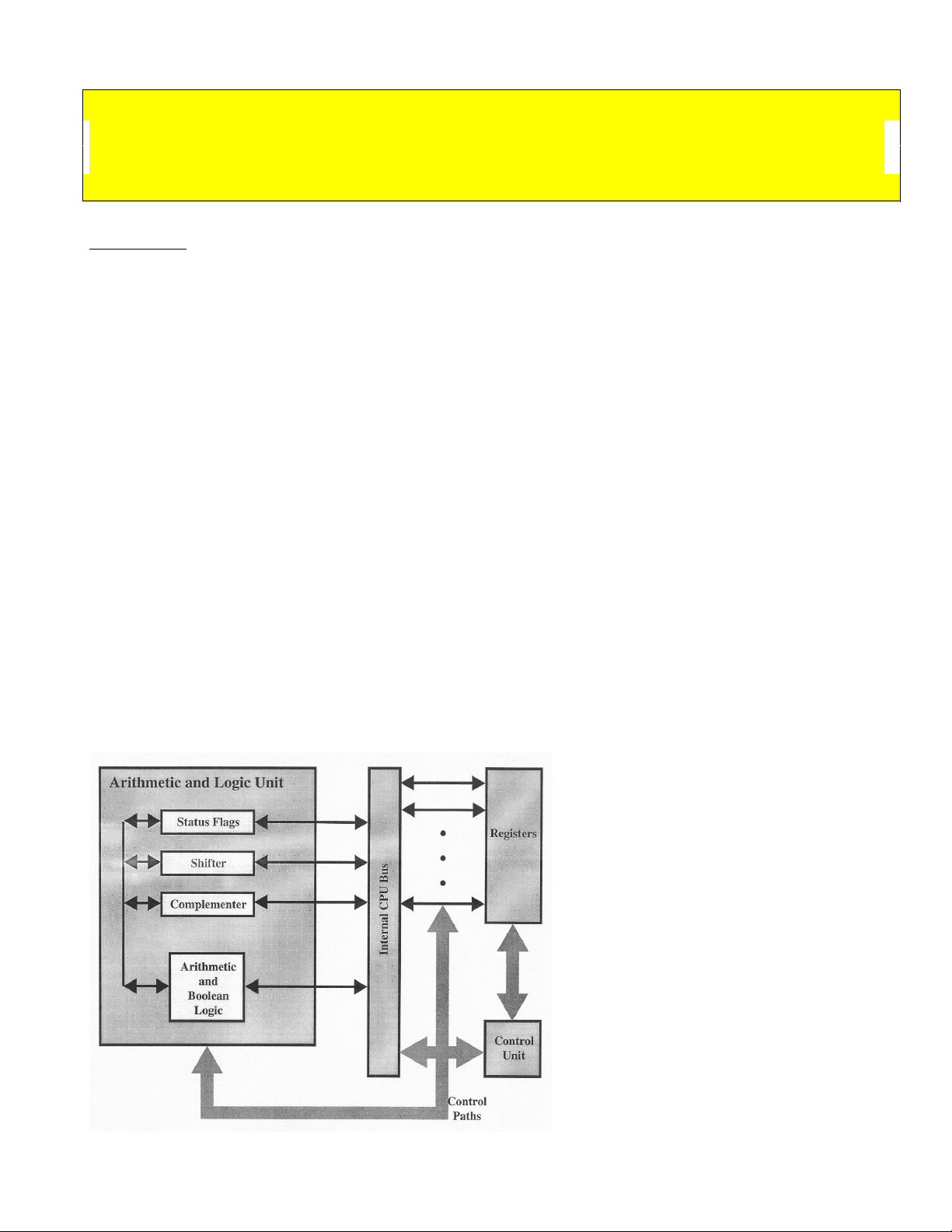
- Execution occurs in a sequential fashion (unless explicitly modified) from one instruction to the next. The Central Processing Unit (CPU) is the computer's brains. All other components in within the computer (I/O system, monitors, etc.) are there basically to bridge the gap between the user and the CPU. The CPU itself consists of three major components: a register set, an arithmetic/logic unit, and a control unit. These three components typically communicate (exchange data) amongst themselves using local buses. The CPU communicates with the I/O system and memory system using one or more system level buses, local buses, or expanded local buses. The typical CPU configuration for a simple computer is shown in Figure 1. Figure 1. High-level view of CPU
When the CPU exchanges data with the memory module it will typically make use of two internal registers: a memory address register (MAR) that specifies the address in memory at which the next read or write operation will occur, and a memory buffer register (MBR) that either holds the data that will be written into the memory location or will receive the data from the memory location. The CPU will have many such registers, such as an I/O address register (I/OAR) which specifies a particular I/O device, and an I/O buffer register (I/OBR) that will be used for the exchange of data between an I/O device and the CPU. We’ll examine each of the three components of a CPU briefly and then go back and look at each in more detail once some background information is covered. The ALU (Arithmetic/Logic Unit) All computers have functional units that perform the arithmetic, logical, and shift operations required by the instruction set (we’ll use the terms functional unit and ALU interchangeably). All the other components of the system are there mainly to bring data into the functional unit for it to process and then to take it back out. In a sense, we have reached the core of a computer in the functional unit. Some computers have a single functional unit, the ALU, but more advanced CPUs will have several independent functional units. Functional units themselves may contain functional units. Early microprocessors that contained a single ALU were often augmented with a special floating-point unit (FPU) on another chip called a math-coprocessor. Intel's early math coprocessor family (x87 line) is shown in Appendix C. Current technology incorporates these coprocessors into the main chip. Typically the ALUs will communicate with the control unit via dedicated control and status buses. Local data buses will carry data to and from the CPU’s registers. Some computers have special floating-point coprocessors to implement more complex arithmetic operations. Floating-point units generally arrange their registers in stacks. Stack oriented floating point units are considered lean and mean. RISC (Reduced Instruction Set Computers – we’ll see these later) commonly have several independent functional units that implement different types of instructions, such as branch processing. It is quite common for systems with more than one functional unit to employ pipelining techniques to supply the functional units with instructions and data. The overall speed of a von Neumann machine depends largely on the speed of its computational circuitry (in the functional units), so design emphasis is placed on efficient functional units. Data is sent to the functional unit via registers, and the results of an operation performed by the functional unit are returned via storage into a set of registers. These registers are located within the CPU and are connected via signal paths to the ALU. The ALU may also set various flags as the result of an operation. For example, if an addition operation causes an overflow that results in the calculated
Later we will examine some of the features of modern systems that make this sequence of operations much more complex but also more powerful. Figure 3(a) – Simple von Neumann machine with program in memory Figure 3(b) – Fetching instructions and incrementing register values The control unit is responsible for generating the signals that regulate the computer. For the simple system that we are currently considering, the control unit will typically send micro-orders , individual signals sent over dedicated control lines which control individual components and devices. An example might be a control signal that sets or clears a particular status flag. A specific example of this might be a clear carry signal that tells the ALU to clear the addition carry status bit (flag) (see the ALU above). In modern systems, it is much more common that the control unit will generate sets of micro-orders which operate concurrently rather than individual micro-orders. A set of micro-orders issued by the control unit at one time are called micro-instructions. Whenever a computer executes a machine instruction from its instruction set, the control unit issues a sequence of micro- instructions. This sequence of micro-instructions is called a micro-program. Although it is possible for a micro-program to consist of a single micro-instruction, typically it will consist of a sequence of micro-instructions. For example, when an accumulator-based machine executes an ADD instruction, the control unit issues microinstructions for computing the address of the first operand in memory, for reading that memory location and transferring the operand found at that address
into the ALU, for transferring the second operand from the accumulator to the ALU, for adding the two values, and for transferring the result computed by the ALU back into the accumulator. The exact number and type of microinstruction sequences that will be generated by the control unit depends upon many factors including, the complexity of the addressing calculations required and the availability of different types of buses within the machine. There are basically two different types of control units: microprogrammed and conventional. Most of the computers built during the 1970s and 1980s had microprogrammed control units, whereas high-speed systems and RISC processor use the conventional (hard-wired) form. Microprogrammed control units are relatively easy to design and enable the design of complex instruction sets with relatively little cost. They are however, slower than conventional control units, which makes them difficult to use them to generate the control signals that are needed for high-performance or RISC machines. Appendices A and B give an overview of how RISC and CISC processors differ. For many years the general trend in computer architecture and organization has been toward increasing processor complexity; more instructions, more addressing modes, more specialized registers, and so forth. The RISC systems represent a complete departure from than trend. In the mid-1980’s in particular, the debate between RISC and CISC architectures was a strongly debated topic in the computer architecture world, with proponents on both sides extolling the virtues of their architecture. In recent years, this debate has, for the most part, died away. This is because there has been a gradual convergence in the two architectures. As chip densities and hardware speeds have increased, RISC systems have become more complex (trend is to become more CISC-like). At the same time, in order to gain maximum performance, CISC systems have adopted strategies such as increasing the number of general purpose registers and emphasizing and refining instruction pipelines (trend is to become more RISC-like). A case in point would be Intel’s Pentium family of processors, whose instruction set is very much CISC- oriented, yet the processor employs many RISC-like strategies, such as out-of- order execution, instruction pipelining, multiple functional units, and many RISC- style commands. CPU Operations and Instruction Sets Instructions are the basic units for telling the microprocessor what to do. To execute a single instruction the microprocessor must carry out hundreds, thousands, or even millions of logic operations. The instruction, in effect, triggers a cascade of logical operations. How this cascade is controlled marks the great divide in microprocessor and computer design.
simpler instructions. Although each instruction would take longer to execute because of the microcode, programs would need fewer instructions overall to accomplish the same task. Moreover, adding more instructions could further boost this speed gain. One result of this is that most typical PC microprocessors have 7 different subtraction commands. The Register Set The register set is the third of the three major components of a CPU that we will examine individually. A computer system employs a memory hierarchy. At higher levels in the hierarchy, the memory is faster, smaller (in total number of bytes), and more expensive per bit. Within the CPU itself, there is also a memory hierarchy. The register set is at the highest level followed by main memory followed by the first of possibly several levels of cache memory. The registers in the CPU serve two primary functions:
- User-visible registers: These enable the machine language (or assembly language) programmer to minimize main memory references by optimizing the use of the registers. User visible registers fall into four general categories: i) General purpose registers : may be assigned a variety of functions by the programmer. Some may be dedicated to floating-point or stack operations. In some machines the general purpose registers may be used for addressing functions (i.e., register indirect, displacement values). ii) Data registers : Can be used only to hold data values and cannot be used in the calculation of an operand address. iii) Address registers : may be somewhat general purpose (as far as addressing modes are concerned) or they may be devoted to a particular addressing mode. For example, some address registers may be index registers for indexed addressing modes, others may be addresses to the top of stacks for machines which support user-visible stack addressing. On machines that support segmented addressing, segment registers will hold the base address of the segment. iv) Condition code registers : (also referred to as flags) hold the condition code bits set by the CPU to indicate the status of operations it has performed. For example, an arithmetic operation may produce a negative, zero, positive, or overflow result. A condition code will be set by the CPU to indicate which result is produced, this can be tested by examining the condition code for the operation.
- Control and status registers: These are used by the control unit to control the operation of the CPU and also by privileged operating systems programs to control the execution of programs. The exact number and use of these registers will vary from machine to machine, but the following list is a fairly complete set of control and status registers that would be found on the average machine: i) Program counter (PC): contains the address of the next instruction to be fetched for execution. ii) Instruction register (IR): contains the address of the instruction most recently fetched and currently in execution (most likely). iii) Memory address register (MAR): contains the address of some location in memory. iv) Memory buffer register (MBR): contains the word of data to be written to memory (usually to the address contained in the MAR), or the word most recently read from the memory. v) Program status word (PSW): All CPUs include a register (or a set of registers) that contain status information about the processor. Usually this register contains many condition codes as well as status information. This register will contain an indication if the processor is executing in a supervisor or user mode (certain instructions from the instruction set can only be executed when the processor is in supervisor mode, similarly, certain memory areas can only be addressed while in supervisor mode). An indication of the interrupt status (enabled/disabled) as well as arithmetic operation conditions will be included in this register. Depending upon the machine several other control registers may be present, such as a register which hold pointers to PCBs (process control blocks). Since the CPU is expected to work closely with an operating system, much of the design of the control and status registers is focused on providing proper support for the operating system. There is often not a clear distinction between these two sets of registers. For example, on many machines the PC register (the program counter register) is user-visible, on other machines it is not. The I/O System Even though the I/O system is not part of the CPU, it plays an important role in the overall performance of a computer system. We will briefly discuss the I/O system and examine its role in the interaction with the CPU.
CPU-controlled I/O The designers of early computer systems paid little attention to I/O processing, and the CPU directly controlled the I/O devices using very simple I/O instructions (remember, the devices weren’t very sophisticated either so the instructions didn’t need to be too complex). Instructions were of the form “Write A to Device N” where A was typically a register address and N designated an I/O device address. The instructions typically transferred one byte or one word at a time. The computers ran one program at a time and each program executed its own instructions for I/O. As computer systems evolved an ever-widening gap between the speed of the CPU and the speed of the I/O devices began to occur, which has become even wider today. The challenge then, has been to find ways to keep the CPU utilization high even though the I/O devices are very slow. Three different solutions have emerged, which are all based upon other developments that have occurred whose potential performance gains have been exploited. These three areas are:
- Multiprogrammed Operating Systems. The operating system loads several different programs into the memory at the same time. The CPU can then execute instructions from one of the programs while another waits for an I/O operation to complete.
- Multi -ported Memory Systems. This type of memory (which we will examine more closely when we look at memory systems) either allow several processors to access the memory simultaneously, or they arbitrate requests for memory cycles amongst the competing processors and I/O devices which allows for memory sharing amongst the processors and I/O devices.
- I/O processors. These special I/O interfaces, which include devices called DMA channels, and peripheral processing units (PPUs), can control the I/O devices without CPU intervention. Memory-mapped I/O Rather than have special instructions for handling I/O, some computers (typically micros and minis) use memory-mapped I/O. In memory-mapped I/O certain specific addresses within the memory space are reserved for controlling the I/O interface device. Essentially the I/O interface devices take the place of a portion of the physical main memory, and the CPU controls them using standard instructions that read and write to memory. For example, if the physical address space of a computer is 64K, the designer may reserve the upper 16K for I/O interface devices. The I/O interface devices decode addresses that appear on the address bus. Each I/O interface device responds to one or more specific I/O port addresses (typically there are control ports, status ports, input ports, and output
ports). I/O port addresses are simply main memory addresses and are mutually exclusive in that no other I/O interface device (or memory) will respond to the same port addresses. A processor that uses memory-mapped I/O requires no special I/O instructions. A store operation to an output port sends the data to the attached I/O interface device, and a load operation from an input port will receive data from an I/O interface device. In fact, the CPU cannot distinguish between a memory access and an access to an I/O interface device. A store operation to a control port will set an I/O command to the interface device, and a load operation from a status port will get status information from the device. To output a value, the CPU simply stores the output value in the correct output port address, and to input a value the CPU loads it from the correct input port address. CPU-controlled I/O and memory-mapped I/O are not exclusive concepts. Computers may have both types of I/O control, the IBM PC was an example. There are a large number of I/O interface devices, including DMA controllers, programmable parallel interfaces (PPIs), and universal asynchronous receiver- transmitters. DMA I/O Hardware devices that directly control the transfer of data to and from main memory are called direct-memory-access controllers. Some systems will have very simple DMA controllers while other systems may have quite powerful DMA controllers. For the simple type DMA controllers, each transfer of data, the CPU sends the DMA controller the memory address for the block of data, the number of bytes to transfer, and the direction of transfer (input or output). The DMA controller then performs the transfer without CPU intervention and interrupts the CPU when the transfer is completed (signaling the CPU that the operation has completed). For simple, single bus systems, the DMA controller will become the bus master during the transfer operation (we’ll see more about this when we discuss the memory system, for now it means that the DMA controller is the only device that can use the bus while it is the master). While the DMA controller is the bus master, the CPU, which is working on some other problem now, may have to wait to use the bus. The DMA controller is said to “steal bus cycles” from the CPU. Cycle stealing refers to any situation in which an I/O device causes the CPU to wait because the I/O device currently has exclusive access to a shared resource. IBM machines are typical of machines that employ relatively simple DMA controllers in the form of channels. In IBM nomenclature, a channel is an I/O processor that executes DMA I/O under the supervision of a channel program. Current channels will employ large amounts of cache memory for data buffering
of the Pentium II and had a 8K L1 data cache and a 8K L1 instruction cache) Both L1 caches in the P2 are 16K. A major architectural difference in the Pentium architecture compared to the x architecture is that the Pentium, Pentium Pro, and P2 have two ALUs for integer calculations and a single FPU (floating point unit). The P3 has to FPUs, one dedicated to the MMX unit and the other shared by the CPU and the Internet Streaming Instruction unit. These additional execution units allow the Pentium family architecture to show super-scalar speed-up over the 486 architecture. P2 and P3 processors contain the MMX unit, which is a special purpose unit (processor) designed to improve the performance of graphic and multimedia software. In the P2 this is done via a set of 57 different instructions tailored to perform small, repetitious operations that are commonly needed in multimedia. The FPU is shared by the main processor and the MMX unit. In the P3 the MMX unit gets its own FPU and the number of MMX instructions has been increased to around 70. The CPU isn't the only microprocessor in most modern systems. There are several coprocessors which handle specific types of tasks such as graphics and video (AGP), 3-D accelerators, DSP (digital signal processors), sound cards, etc. Clocked Logic Microprocessors do not carry out instructions as soon as the instruction code signals reach the pins that connect the microprocessor to the computer's circuitry. Electrical signals do not change state instantaneously, instead they always go through a brief (but measurable) transition period during which the state of all signals (voltage levels) stabilize to their final values. The microprocessor must wait for an indication that all signals are valid, i.e., that it has a valid command to execute. This indication is the ticking of the system clock. At each "tick" of the clock the microprocessor checks the instructions given to it- if it is not already processing an instruction. Early microprocessors could not execute 1 instruction/clock cycle. Many instructions required as many as 100 clock cycles. In current systems, which employ many RISC-like features, many instructions take less than 1 clock cycle to execute via multiple ALUs, pipelined ALUs, and SIMD techniques (inside the MMX units on Pentiums). Clock Multipliers allow the microprocessor circuitry to run faster than the system clock. The system clock is multiplied by the clock multiplier (typically 1.5, 2.0, 2.5, 3.0, etc.) In this fashion the CPU is allowed to operate internally at a rate which is faster than the system clock would allow.
The lack of correspondence between the clock cycles and the instruction execution speed means that the clock speed of the system alone is not a good metric for relating the performance of two different processors. See the example below. Clock speed only gives a reliable indication of relative performance when two identical microprocessors operating at different frequencies are compared. The Advanced Technologies of Modern CPUs Overview Today's higher clock speeds make circuit boards and integrated circuits more difficult to design and manufacture. Designers have a strong incentive to get their microprocessors to process more instructions at a given speed. Most modern microprocessor designs intend to do just that. One way to speed up execution of instructions is to reduce the number of internal steps the microprocessor must take to execute an instruction. Reducing the number of steps can be accomplished with two basic techniques: make the processor more complex so that internal steps can be combined or by making each instruction simpler so that fewer steps are needed. The former technique is the one taken by CISC designers while the latter technique is employed by RISC designers. Another way of reducing the number of clock cycles required to execute a program is to operate on more than one instruction simultaneously. Two basic approaches to operating on more than one instruction simultaneously are: pipelining and superscalar architecture. Both CISC and RISC designs take advantage of these techniques as well as other techniques. Example: Suppose that processor P1 requires an average of six clock cycles per instruction and the system clock runs at 400 MHz. Processor P2 requires an average of two clock cycles per instruction and the system clock runs at 200 MHz. For P1 = 400 MHz / 6 cycles / instruction 67 For P2 = 200 MHz / 2 cycles / instruction 100 Thus, (67 - 100)/67 -50% or P1 is 50% slower than P2 even though it's clock speed is twice as fast as P1.