CPSC 2105 / CPSC 5155 Computer Organization/Architecture
Lab Assignment Modulo–4 Counter
The purpose of this lab is to use a circuit emulation tool to continue our investigation of
simple D flip–flops, to understand better how to use the emulation tool, and to design a
simple “one hot” modulo–4 counter. We begin with a simpler design with two flip–flops.
The Silly Circuit
We begin with a circuit that has two flip–flops and no apparent use. The purpose of this first
exercise is to hook up two D flip–flops in a circuit that demonstrates a few features. The two
flip–flops will be labeled FF1 and FF2. The design specifications are as follows:
FF1 this will be initialized to 1.
It will have input from a switch.
FF2 this will be initialized to 0.
It will have its input from the output of flip–flop 1.
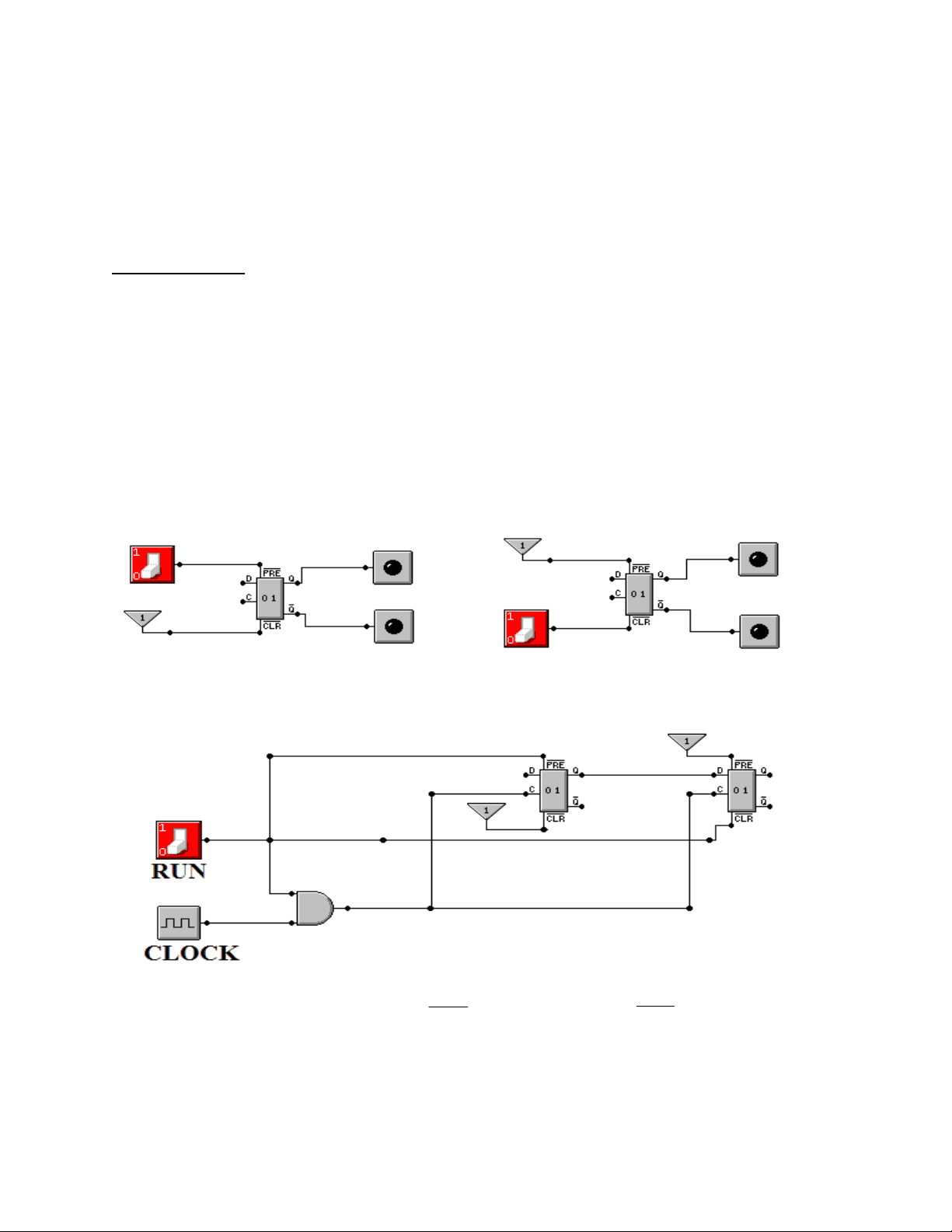
Here is the basic idea for initializing the flip–flops. The circuit on the left shows a flip–flop
that is initialized to Q = 1; this is used for FF1. The circuit on the right shows a flip–flop that
is initialized to Q = 0; this is used for FF2.
RUN = 0 Flip–flop is preset to Q = 1 RUN = 0 Flip–flop is cleared to Q = 0.
The first step of this lab is to lay down the basic structure.
In this figure, we see the following features that will be used in the final circuit.
1. The signal RUN is attached to the
PRE
input of FF1 and the
CLR
input of FF2.
When RUN = 0, FF1 is set to 1 and FF2 is cleared.
2. The signal RUN is also an input to an AND gate used as a clock input to each of
FF1 and FF2. Each receives the clock signal only when RUN = 1.