


ECE 412: Mixed-signal circuit design Homework 6
Due Tuesday (11/19/2007)
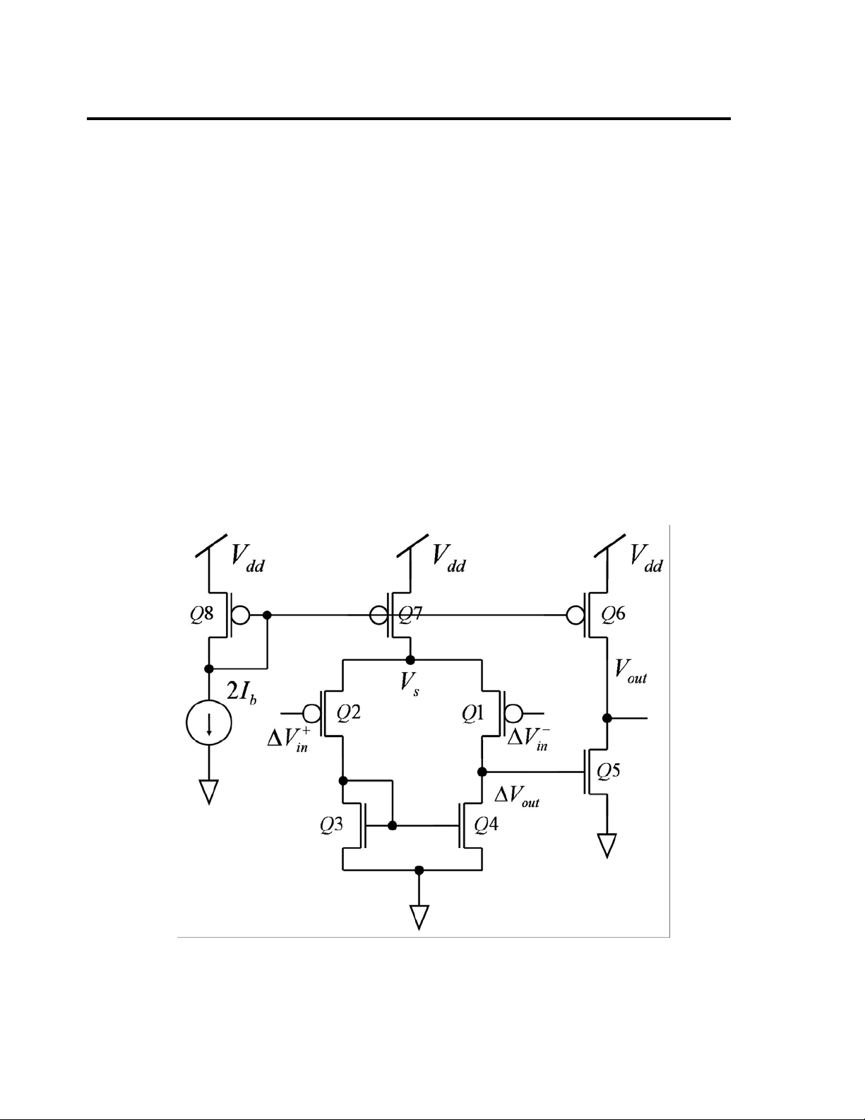
In this assignment you are required to use cadence simulations to design an
operational amplifier (using the circuit in Figure 1) with the following
specifications. You would need to choose the sizes of the transistors in Figure
1 appropriately.
Fig. 1
1. The open loop dc gain of the amplifier should be at least 60dB.
2. The bandwidth of the amplifier should be at least 10KHz.
3. The phase margin should be at least 55 degrees.
Hints: Calculate the gain using small signal analysis. For this you need to know the
approximate values of gmand gd. To match the bandwidth and also the gain
specification you have to choose the correct range of the bias current Ib. To
achieve the phase margin specification follow the steps described in the
frequency compensation slides.