SORTING Circuit
Specification
Function
Design a circuit capable of sorting 2L N-bit numbers.
Optimization
Optimize your circuit for the minimum total execution time. When choosing between two circuits
with the same or very similar execution time, give preference to the circuit with the smaller area.
Interface
Assume the following interface to your circuit:
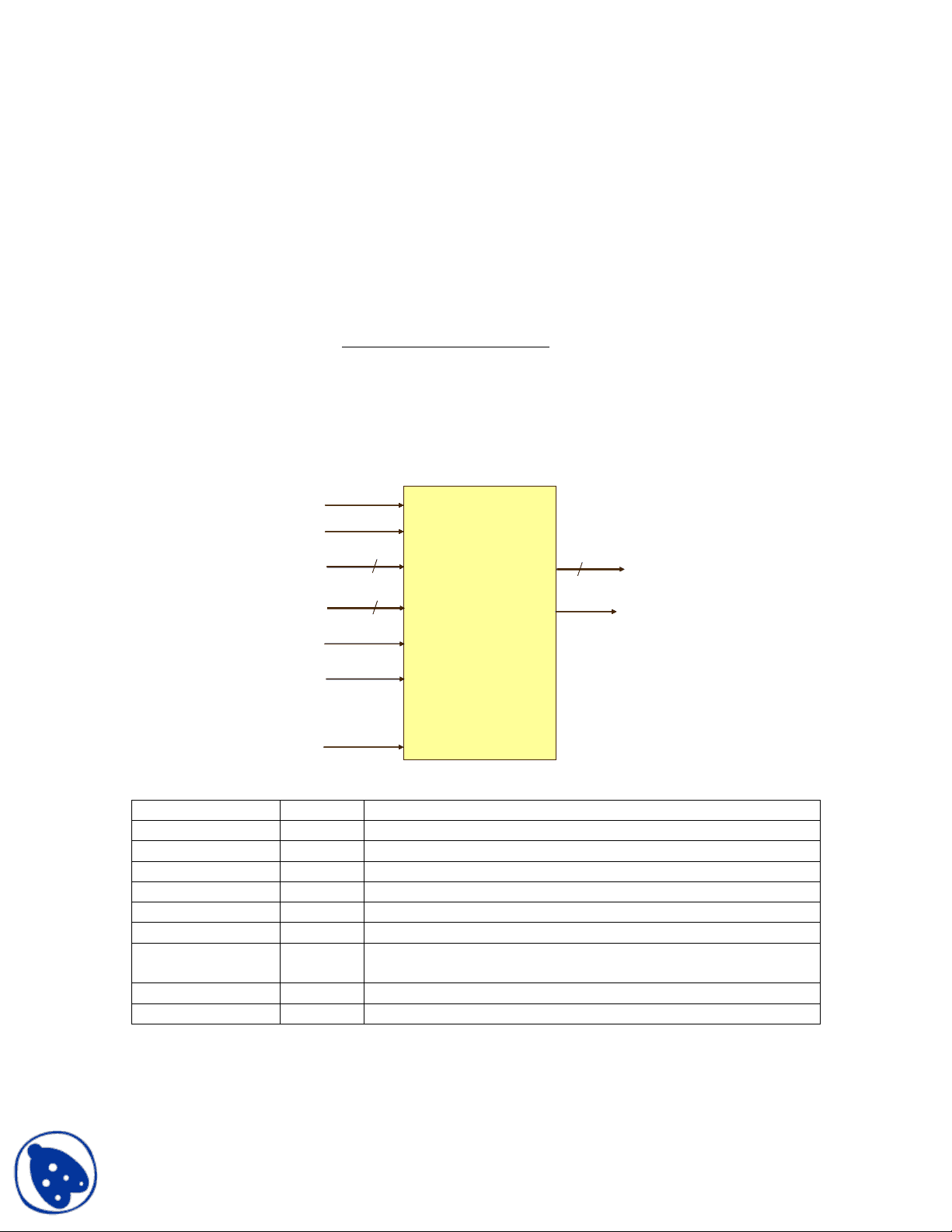
Sort
Clock
Resetn
DataIn
N
DataOut
N
Done
RAdd
L
WrInit
S
(0=initialization
1=computations)
Rd
Sort
Clock
Resetn
DataIn
N
DataOut
N
Done
RAdd
L
WrInit
S
(0=initialization
1=computations)
Rd
Port
Width
Meaning
clk
1
System clock
Resetn
1
System reset – clears internal registers. Active low.
DataIn
N
Input data bus
RAdd
L
Address of the internal memory where input data is stored
WrInit
1
Synchronous write control signal
s
1
Operating mode: 0 = initialization, 1 = computations.
Rd
1
Read enable. 0 = high impedance on the output bus, 1 = valid
output on the output data bus.
DataOut
N
Output data bus used to read results
Done
1
Asserted when all results are ready
docsity.com