Download Tri-State Output -Components and Design Techniques for Digital System - Exams and more Exams Digital Systems Design in PDF only on Docsity!
EECS150, Fall 2002
Midterm
Professor Wawrzynek
85 pts
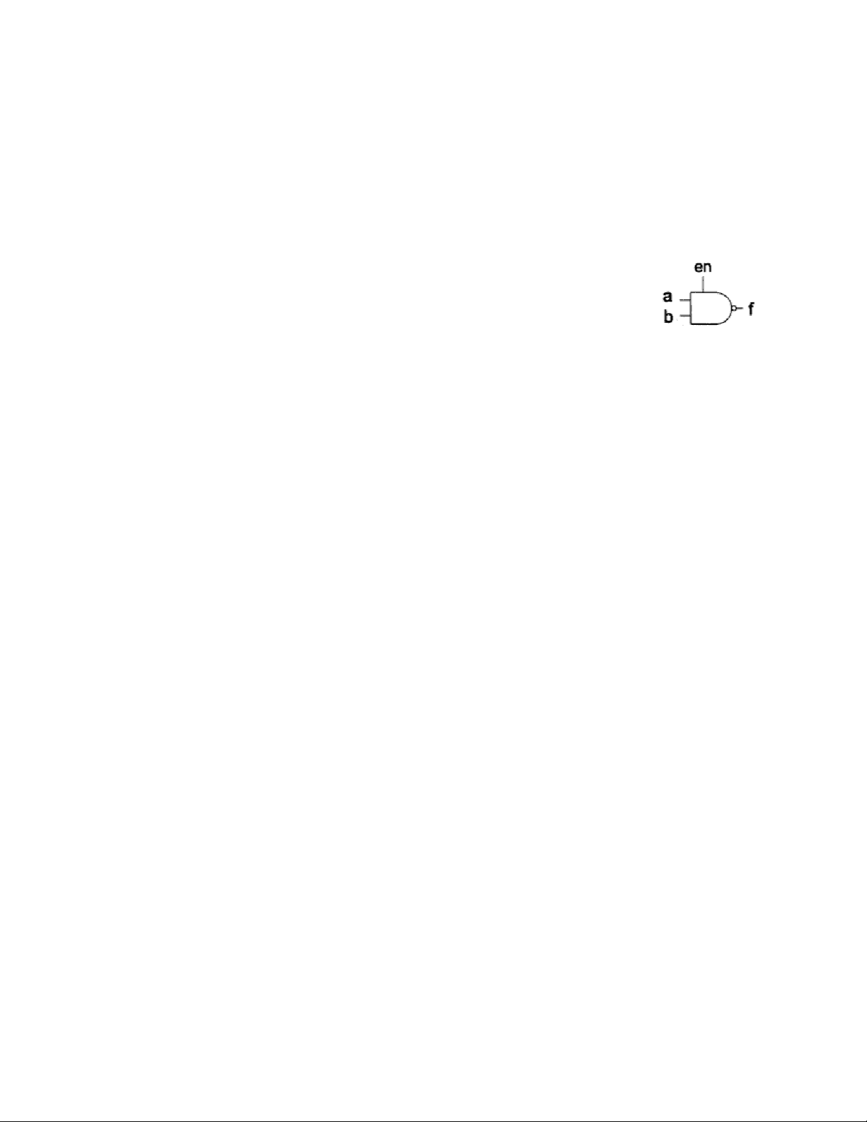
- [5pts] In the space below, draw the CMOS transistor-level diagram for a 2-input NAND-gate with tri-state output. Inputs a , and b are the normal NAND inputs; en controls the “state” of the output as in a tri- state buffer (these are the only signals available – if you need more then add circuitry to generate them). Use as few transistors as necessary. Label all inputs and outputs as with the symbol shown to the right.
- [5pts] Consider the D-type edge-triggered flip-flop shown below.
a) Assuming zero setup and clock-to-Q delay, draw the waveform for the signal at node Q.
Q
b) What is the function of the X signal?
- [10pts] Consider the design of a parallel-to-serial converter circuit shown to the right. The circuit accepts a clock signal, CLK , a 4-bit wide data word, X , a load signal, LD , and a control signal named order. On the cycle when loading X , and for the following 3 cycles, if order =0 then the bits of X will appear at y least significant bit first. If order =1 then the bits of X will appear at y most significant bit first. After the bits of X have been sent out, zeros appear at that output on subsequent cycles.
Picking your components from simple gates, flip-flops, and multiplexors, draw a circuit that implements this function. Minimize the number of flip-flips. Label every input and output clearly, and show which boxes are FFs, with a small triangle on the CLK input. Label any mux data inputs with “0” and “1”.
X LD
order CLK
y
- [6pts] Consider the design of a 2-bit carry ripple adder (constructed in the usual way by cascading full-adder cells). Assume that the full-adder cells are implemented with nothing other than 2-input AND, OR, and XOR gates. a) Draw the gates and the connections involved in the critical path through the circuit:
b) What is the value of the critical path in units of gate delays, assuming each gate introduces one unit of delay, for an n-bit carry ripple adder?
- [8pts] A theorem from Boolean algebra states that any function X of variables a,b,c, ... can be expressed as:
X = a ( Y(b,c, ...) ) + a’( Z(b,c,...) ).
Using algebra, show that the following function can be implemented with 2-to-1 multiplexors only (no other gates or inverters). Inputs to the circuit are the variables a,b,c,... and the constants 0 and 1:
X = a’b’c’d + ag’h + ag + a’b’ce + a’bf’. Draw the resulting circuit.
- [5pts] A function F is defined by the true table below. Write F’ in reduced product-of- sums form using a K-map.
a b c d F 0 0 0 0 0 0 0 1 0 0 1 0 0 0 1 1 0 1 0 0 0 1 0 1 0 1 1 0 0 1 1 1 1 0 0 0 1 0 0 1 1 0 1 0 1 0 1 1 1 1 0 0 1 1 0 1 1 1 1 0 1 1 1 1
ab
cd
- [5pts] A bit-serial adder is a finite state machine that forms the sum, in n cycles, of two n- bit binary numbers, A and B, by accepting the bits of A and B, a0 and b0, a1 and b1, etc., one pair per cycle, least significant bit first, and outputting the sum bits, s0, s1, s2, one per cycle. The input signal, END, in used to separate one sum operation from the next. On the cycle after the final two data bits of A and B are fed into the circuit, the END input is asserted. As long as the END input is equal 1, the machine waits – holding the output at constant value zero. On the first cycle of the next pair of data words the END input is set to zero and the sum operation begins.
Draw the state transition diagram for a Moore-style finite state machine implementing the bit- serial adder. Make sure to space your state bubbles well apart to leave room for the arcs. Remember to clearly label the states with their outputs, and the input values for state transitions.
- [10pts] Given the below state transition diagram, draw the circuit diagram for the one- hot encoded implementation. Use flip-flops and AND or OR gates of any number of inputs. Use bubbles to indicate inversion when necessary. Assume that the flip-flop have both set and reset inputs (as indicated below). Don’t forget the output signal.
- [10pts] Short answer.
a) [1pt] Moore’s law says that the number of transistors on an integrated circuit double every how many months?
b) [1pt] A way to lower the cost per part (manufacturing costs) of a device at the expense of higher NRE (non-recurring engineering) costs would be to switch from an FPGA implementation to an implementation using what?
c) [1pt] True or false. Clock skew can lead to increased maximum clock frequency over a circuit with no clock skew.
d) [1pt] The Xilinx Virtex FPGA CLB (with its two slices) can implement any Boolean function of up to how many variables?
e) [1pt] In 2 literals x + x’y =
f) [1pt] How many different functions can a 3-LUT impelement?
g) [1pt] Module AndOr (f, a, b, c, d); input a, b, c, d; output f; // fill in dataflow description using continuous assignment for f=ab + cd
endmodule
h) [1pt] Module AndOr (f, a, b, c, d); input a, b, c, d; output f; // fill in here for f=ab + cd by primitive gate instantiation
endmodule
i) [2pt] Module DFFwithSetAndReset (Q, CLK, D, S, R); input CLK, D, S, R; output Q; reg Q; // fill behavior description for positive edge triggered flip-flop with // synchronous (happens on rising edge of clock) set (s) and reset (r). // Set takes priority over D, Reset takes priority over set.
endmodule