Download Computer Engineering Final Examination for Cmpe 2030 A, June 10th, 1999 and more Exams Computer Science in PDF only on Docsity!
Cmpe 2030 A
Introduction to Computer Engineering
Final Examination
June 10th, 1999
There are 15 questions and 11 pages including the cover sheet and two blank work sheets and three data sheets. Please make sure that you have all of them. This examination is closed text- book. No calculators, class notes or any material is allowed!
- Please write legibly. Use the work sheets if you need to.
- Please show all of your work
- State any assumptions you feel you have to make or ask for clarification
- Keep in mind it is difficult to give partial credit without written material. Please make sure you document any partial solutions.
- All questions carry equal points. Plan your work!
6.The exam is 2 hours and 50 minutes.
Name:_________________________________________________
Student Number:_________________________________________
Question Points Graded 1 15 2 15 3 20 Total 50
- Provide a switch level implementation of the following expression using n-type and p-type switches.
F = A ⊕ B
3 Implement the following expression using only NAND and NOT gates. Use the mixed logic notation we have used in class. Do not assume that the complements of the inputs are avail- able. Do not simplify the expression. Provide the number of transistors in the implementa- tion.
Transistors = ____________
F = ( A + B ) C + AC + BCD
4 This questions deals with logic minimization using K-Maps.
4 (a) Simplify the following expression algebraically to a sum of products form.
4 (b) Fill in the K-Map for the preceding function.
F = A + C + BC D ( + B )
Function _______________________________________
A
C
B
D
CD
AB
5(a) Draw the gate level implementation of a 2:1 multiplexor. Clearly label all of the control, input, and output signals.
5 (b) Show how you can construct a 4:1 multiplexor using 2:1 multiplexors. Clearly label all control, input, and output signals. Clearly show all of the connections between multiplex- ors.
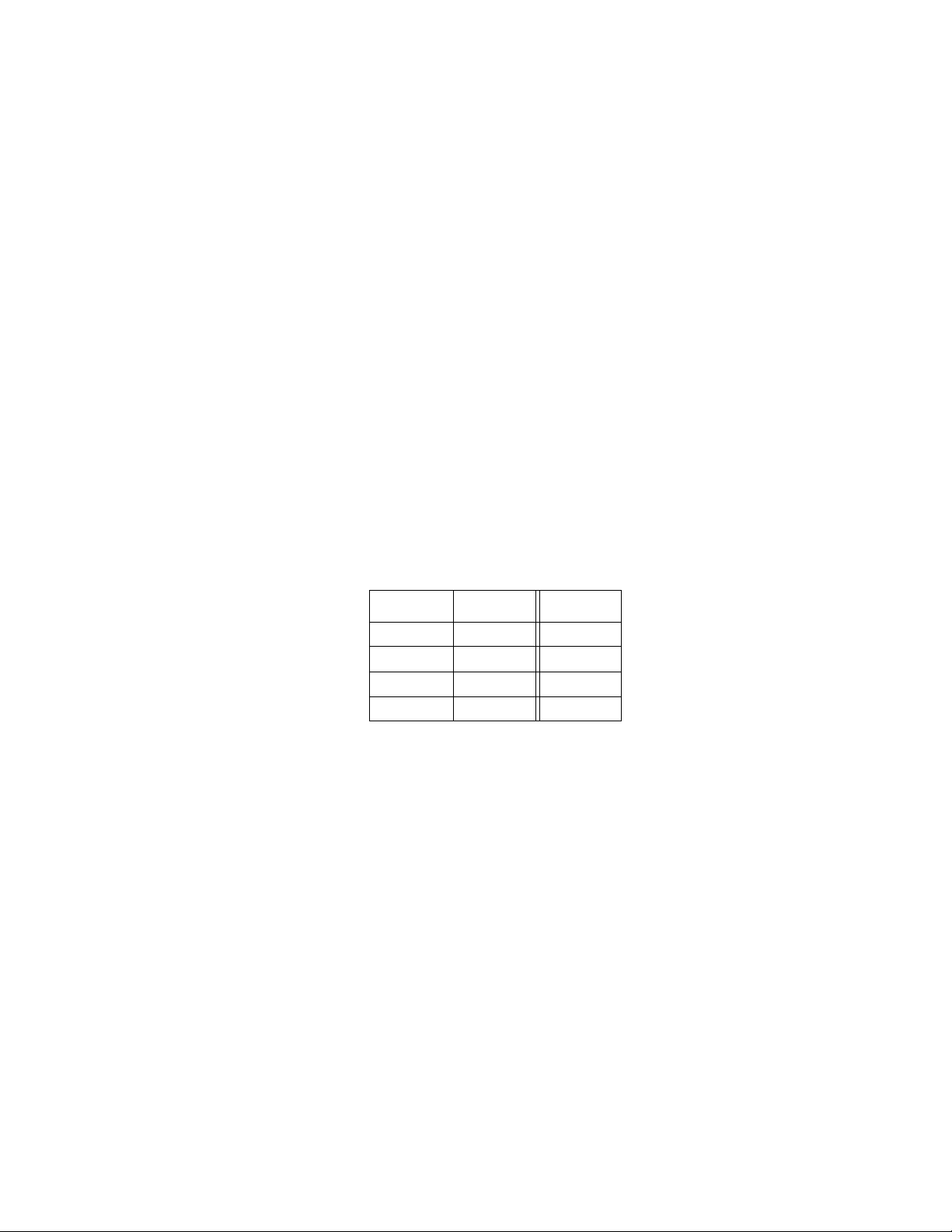
- Consider the boolean function specified with the truth table shown below.
Implement this function using a decoder. Clearly label all signals including the inputs, out- put and multiplexor select lines.
A B C Out 0 0 0 1 0 0 1 1 0 1 0 1 0 1 1 0 1 0 0 0 1 0 1 0 1 1 0 1 1 1 1 1
- Show the heaxadecimal value of the IEEE 754 floating point representation of -1.0.
8 (a) What is the result to of the following floating point operation? The numbers are shown in complete normalized IEEE 754 form: 1.101 x 2^129 + 1.01 x 2^122
- Draw the gate level implementation of a D latch.
9 (a) Complete the timing diagram below for the circuit shown below.
phi
phi
Input
B
transparent latch
transparent latch
transparent latch
transparent latch
input
A B
phi1 (^) phi2 phi1 phi
A
10 (c) Design the counter and show the implementation. You may use any technique you wish.
11 (a). What is the difference between memory based on DRAM cells and memory based on SRAM cells?
11 (b) The following illustrates the internal organization of a 4M x 4 memory chip. Assuming that the array is a square, i.e., has the same number of rows and columns answer the follow- ing with respect to this design.
A Array
R o w D e c o d e
I/O
Column Decode
CS
WE
D
of bits reuqired for row decode __________________
Expression (in terms of CS and WE) for reading from the array _______________
- Consider the following SPIM program. The data segment starts at 0x10010000 and the text segment starts at 0x00400000.
12 (a) What is the final value of the contents of memory location labeled result?
12 (b) What are the values of the labels str and result?
.data label: .word 0, 1, 2, 3, 4, 5, 6, 7 str: .asciiz “Final” .align 2 result: .word 4
.text addi $t5, $0, 8 add $t0, $0, $ begin: lw $t1, label($t0) add $t2, $t1, $t addi $t0, $t0, 4 addi $t5, $t5 - bne $t5, $0, loop sw $t2, result($t0) li $v0, 10 syscall
result _______________
str ___________________
result ___________________
12 (c) Assume that the register $sp points to the top of the stack, this location contains the value on the top of the stack. Write a short SPIM program that pushes the contents of reg- ister $t0 onto the top of the stack.
- Consider the multicycle datapath shown overleaf.
14 (a) Draw the state machine for the control of this datapath. Clearly label the function of each state. The state machine should correspond to the implementation of the following instructions: add, sub, beq, lw, sw.
14 (b) Write the complete microcode for implementing the branch instruction.
cycle X Y Z rwe
imm en
imm va
au en a/s
lu en lf
su en st
ld en
st en r/w msel Descr 1 2 3 4 5 6 7 8 9
10