Download Understanding Flip-Flops in Sequential Logic: SR Latches, D Latches, and Flip-Flops and more Study notes Computer Science in PDF only on Docsity!
6. Sequential Logic – Flip-Flops
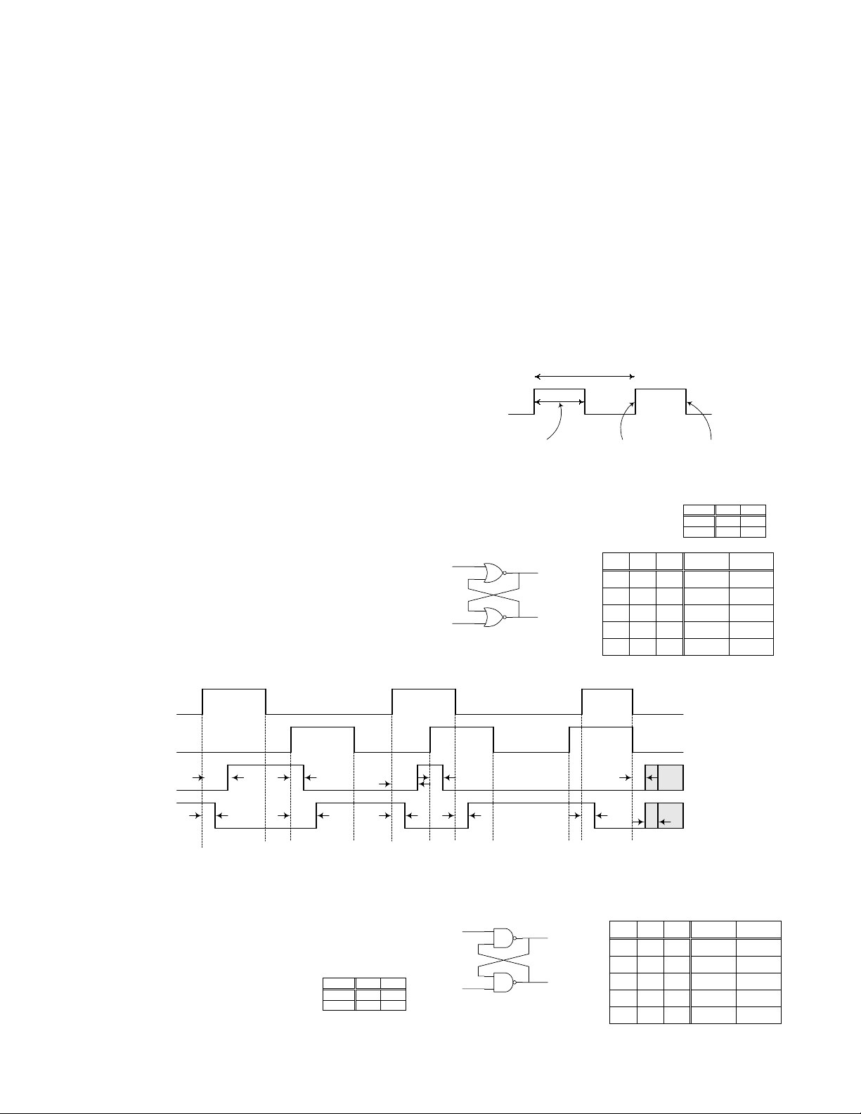
Combinatorial components : their output values are computed entirely from their present input values. Sequential components : their output values are computed using both the present and past input values. In other words, their outputs depend on the sequence of input values that have occurred over a period of time. This dependence on the past input values requires the presence of memory elements. The values stored in memory elements define the state of a sequential component. Since memory is finite, therefore, the sequence size must always be finite, which means that the sequential logic can contain only a finite number of states. So sequential circuits are sometimes called finite-state machines. Sequential circuits can be a asynchronous or synchronous. Asynchronous sequential circuits change their state and output values whenever a change in input values occurs. Synchronous sequential circuits change their states and output values at fixed points of time, which are specified by the rising or falling edge of a free-running clock signal. Clock period is the time between successive transitions in the same direction, i.e., between two rising or two falling edges. Clock frequency = 1/clock period Clock width is the time during which the value of the clock signal is equal to 1. Duty cycle is the ratio of clock width and clock period. Active high if the state changes occur at the clock's rising edge or during the clock width.
Active low if the state changes occur at the clock's falling edge.
Latches and flip flops are the basic storage elements that can store one bit of information.
6.1 SR Latch
The simplest memory element. Consists of two cross-coupled NOR gates. Inputs S (set) and R (reset) are normally 0. Both active high. Asserting S (setting S=1) will make output Q=1. Asserting R (setting R=1) will make Q=0.
t 0 t 1 t 2 t 3 t 4 t 5 t 6 t 7 t 8 t 9 t 1 0
4 1. 4 1. 4 1. 4
4
4
8 1. 4 1. 4
8
8
S
R
Q
Q '
One problem inherent in the SR latch is the fact that if both S and R are disasserted at the same time, we cannot predict the latch output (as in t10).
The SR latch can also be implemented with NAND gates. S and R are normally 1. They are active low.
C l o c k w i d t h R i s i n g e d g e F a l l i n g e d g e
C l o c k p e r i o d
Q '
Q
S
R
1
0
0 1
Q
Q '
S
R
S R Q Qnext Q'next 0 0 0 0 1 0 0 1 1 0 0 1 x 0 1 1 0 x 1 0 1 1 x 0 0
nand 0 1 0 1 1 1 1 0
nor 0 1 0 1 0 1 0 0
S R Q Qnext Q'next 1 1 1 1 0 1 1 0 0 1 1 0 x 0 1 0 1 x 1 0 0 0 x 1 1
6.2 SR Latch with Enable
Similar to the SR latch but with the extra control input C which enables or disables the operation of the S and R inputs. When C=1, the gated SR latch operates as an SR latch. When C=0, S and R are disabled and the circuit persists in the preceding state.
6.3 Gated D Latch
D latch ensures that inputs S and R never equal to 1 at the same time. Also SR latches are useful in control applications where we often think in terms of setting or resetting a flag to some condition. However, we often need latches to store bits of information and a D latch may be used in such an application. Gated D latch is constructed from a gated SR latch with an inverter added between the S and the R inputs and use a single D (data) input.
The C (control) input is active high in this design but can also be active low. When the C input is asserted, the Q output follows the D input. In this situation, the latch is said to be “ open ” and the path from D input to Q output is “transparent”; the circuit is often called a transparent latch for this reason. When the C input is negated, the latch “ closes ”; the Q output retains its last value and no longer changes in response to D.
Latches are often called level-sensitive latches because they are enabled and transparent whenever C is asserted.
Method 2: Gated D latch can also be implemented using a multiplexer.
n e g a t i v e l a t c h D p a s s e s t o Q w h e n C = 0
0 1 sy
D Q
C
p o s i t i v e l a t c h D p a s s e s t o Q w h e n C = 1
0 D 1 sy Q C
- 0 2. 0
C
D
Q 4. 0
- 0
ts e t u p t (^) h o l d D e l a y t h r o u g h o n e A O I g a t e s i s 2. 0
Problem with the D latch: there is a (shaded) window of time around the falling edge of C when the D input must not change. This window begins at time tsetup before the falling (latching) edge of C; tsetup is called the setup time. The window ends at time t (^) hold afterward; thold is called the hold time.
2
2
Q '
Q
S
R
C
2
(^2) Q
Q '
D
C
1
1
1
0
Q
Q '
D
C
C S R Q Qnext 0 x x 0 0 0 x x 1 1 1 0 0 0 0 1 0 0 1 1 1 0 1 x 0 1 1 0 x 1 1 1 1 x NA
C D Q Qnext 0 x 0 0 0 x 1 1 1 0 x 0 1 1 x 1
nor 0 1 0 1 0 1 0 0
Name FF Symbol
Characteristic (Truth) Table (^) State Diagram / Characteristic Equations Excitation Table
SR Q
Q '
S C l k R
The triangle indicates that the ff is triggered by the rising edge.
S R Q (^) next 0 0 Q 0 1 0 1 0 1 1 1 NA
Q = 0 Q = 1
S R = 0 1
S R = 1 0
S R = 0 0 o r 1 0
S R = 0 0 o r 0 1
Q (^) next = S + R’Q SR = 0 *
Q Q (^) next S R 0 0 0 X 0 1 1 0 1 0 0 1 1 1 X 0
JK
Q
Q '
J C l k K
J K Qnext 0 0 Q 0 1 0 1 0 1 1 1 Q’
Q = 0 Q = 1
J K = 0 1 o r 1 1
J K = 1 0 o r 1 1
J K = 0 0 o r 1 0
J K = 0 0 o r 0 1
Q (^) next = J’K’Q + JK’ + JKQ’ = J’K’Q + JK’Q + JK’Q’ + JKQ’ = K’Q(J’+J) + JQ’(K’+K) = K’Q + JQ’ *
Q Q (^) next J K 0 0 0 X 0 1 1 X 1 0 X 1 1 1 X 0
D
Q
Q '
D C l k
D Q (^) next 0 0 (^1 1) Q = 0 Q = 1
D = 0
D = 1
D = 1
D = 0
Q (^) next = D
Q Q (^) next D 0 0 0 0 1 1 1 0 0 1 1 1
T
Q
Q '
T C l k
T Qnext 0 Q 1 Q’ (^) Q = 0 Q = 1
T = 1
T = 1
T = 0
T = 0
Q (^) next = TQ’ + T’Q = T ⊕ Q
Q Q (^) next T 0 0 0 0 1 1 1 0 1 1 1 0
* SR
0 1
0 0
1 0
0 0
0
1
Q 0 1
4 5
1 1 1 0
x 1
x 1
3 2
7 6
S R S R ' Q
* JK
0 1
0 0
1 0
0 0
0
1
Q 0 1
4 5
1 1 1 0
1 1
0 1
3 2
7 6
J K
K ' Q
J Q '
The characteristic table is a shorter version of the truth table, that gives for every set of input values and the state of the flip-flop before the rising edge, the corresponding state of the flip-flop after the rising edge of the clock. It is used during the analysis of sequential circuits.
The c haracteristic equation is just the functional expressions derived from the characteristic (truth) table. It formally describes the functional behavior of a latch or flip-flop. They specify the flip-flop’s next state as a function of its current state and inputs.
The excitation table gives the value of the flip-flop inputs that are necessary to change the flip-flop’s present state to the desired next state after the rising edge of the clock signal. It is obtained from the characteristic table by transposing input and output columns. It is used during the synthesis of sequential circuits.
Some flip-flops have asynchronous inputs that may be used to force the flip-flop to a particular state independent of the CLK and D inputs. These inputs typically labeled PRS (preset) and CLR (clear), behave like the set and reset inputs on an SR latch.
Q
Q '
D C l k
P R S
C L R
2
2
Q
Q '
D
C
P R S
C L R
A commonly desired function in D flip-flops is the ability to hold the last value stored, rather than load a new value, at the clock edge. This is accomplished by adding an enable input, called EN or CE (clock enable) through a multiplexer.
Q
Q '
D C l k
D
E N
C L K
Q
Q '
Q
Q '
D C l k E N
nor 0 1 0 1 0 1 0 0
D EN CLK Q Q’
0 1 Ç 0 1
1 1 Ç 1 0
x 0 Ç last Q last Q’ x x 0 last Q last Q’ x x 1 last Q last Q’